Relay Logic Projects
Return to Home
Return to Projects
Interested in building relay logic circuits? Consider buying Catahoula Technologies Relay Logic Modules and Catahoula Technologies 4-digit 12-hour relay nixie clock.
In the years since I documented my adventures in relay computing with the Basic Relay Computer and Relay Computer Two projects, I had been contacted over the years by visitors who were interested in building relay-based digital circuits to learn and understand logic functions, binary arithmetic, and how it scales to more complex designs. I thought it would be interesting to revisit the idea by designing several 4-bit PCB modules with similar modular functionality as the decades-old CD4000 series CMOS integrated circuit chips to serve as basic digital building blocks for new relay circuits.
Relay Logic Basics
Relay Logic Level Definition
All modern solid-state CMOS logic gates are derivatives of a basic CMOS inverter comprised of a PMOS and NMOS transistors.
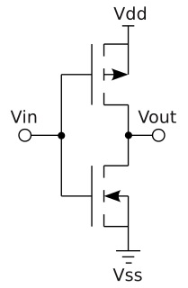
In the above inverter circuit diagram, a PMOS turns on when its gate driven by Vin is driven to 0V so Vout gets driven to Vdd, which is the inverse of Vin hence the circuit is an "inverter." When Vin is driven to Vdd, the PMOS turns off because its gate to source voltage Vgs = 0V. Conversely, the NMOS turns on when its gate driven by Vin is driven to Vdd so Vout gets driven to 0V (again, the inverse of Vin), and turns off when the gate is driven to 0V because its Vgs = 0V. By adding more NMOS and PMOS in parallel or series, more advanced logic circuits such as NAND, NOR, and flip flops could be constructed.
The key takeaway with CMOS logic design is a '0' = Ground and a '1' = Vdd. Any voltage level in between the '0' and '1' thresholds are indeterminate and could be interpreted as either a '0' or a '1'. For this reason, reliable digital logic design always ensures signals are reliably within the well defined regions of '0' or '1' to function correctly.
With relays, there are at least two ways to define a '0' and '1' that I have realized since building Relay Computer Two.
- CMOS style method - '0' = Ground and '1' = Vdd
- "Floating zero" method - '0' = no connection and '1' = Vdd.
- "Floating one" method - '0' = Ground and '1' = no connection is a theoretical alternative to the "floating zero" method that I have not seen implemented by anyone but the principle is the same as a "floating zero" method in that a digital state is defined with a no connection.
Relay Combinational Logic
Combinational logic refers to circuits whose outputs are a direct function of its input with no time sensitivity (i.e. no latch or flip-flop storage). The following diagram illustrates different methods for building logic gates.
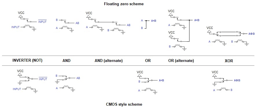
A binary adder is constructed from half and full adders. A half adder relies on a XOR gate to produce the sum and an AND gate for the carry output. Using a floating zero method, a half adder could use up to 4 SPDT relays, but the design could be simplified into a single 4PDT relay as used in Relay Computer Two. With CMOS style logic, a half adder only needs 2 SPDT relays or 1 DPDT relay because the XOR gate is very easy and cheap to do as used in Basic Relay Computer. A full adder is essentially two half adders put together to include a carry input. The full adder will need twice as many relays in the floating zero scheme (two 4PDT), but still remains at two relays with CMOS style logic if the relay size is doubled from SPDT to DPDT. 4PDT relays are generally harder to find and cost more than SPDT or DPDT relays so the floating zero scheme is less appealing.
Relay Sequential Logic
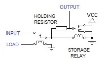
Sequential logic refers to circuits that contain latch or flip-flop storage so their outputs are a function of inputs and past inputs. The following diagram illustrates a 1-bit latch design using a "floating zero" method as used in Relay Computer Two: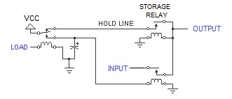
The way this latch works is when LOAD is driven high, the HOLD LINE is released so the storage relay in the upper right cannot self-latch and will release. Meanwhile, the relay at the bottom will connect the INPUT to the OUTPUT and drive the storage relay to a new state. The falling edge of LOAD is when INPUT is captured and stored because the HOLD LINE will go high and allow the storage relay to self-latch if it was actuated by the INPUT signal. If the INPUT is off (floating) on the falling edge of LOAD, the storage relay is off and will latch a '0' by outputting nothing. However, there are a couple shortcomings with this design:
- The output is not actually floating because there is still a relay coil resistance between OUTPUT and ground. Depending on how the OUTPUT is used with other logic circuits, this could result in many headaches as I encountered on Relay Computer Two. Of course, you could use a DPDT relay and have the OUTPUT connect to either VCC or nothing to adhere strictly to the "floating zero" requirement.
- This circuit is actually a latch rather than a flip-flop. When LOAD is high, the latch is in a transparent state passing through INPUT to OUTPUT. When LOAD is low, the latch stores the last state of OUTPUT. Once you start building circuits that require feedback such as a program counter where the value is incremented by 1 and fed back to the register, then you need a clock edge sensitive flip flop rather than a latch. The reason is because when the latch is in transparent mode, an increment logic would end up connecting its outputs back to its input and run haywire.
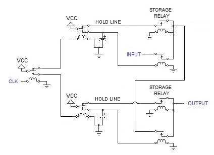
When CLK is low, the upper latch is transparent and the lower latch is in storage mode. INPUT is passed through to the input of the lower latch. When CLK rises, the upper latch stores INPUT and the lower latch becomes transparent passing the stored INPUT value to the OUTPUT. But more importantly, if INPUT changes after CLK is high, it does not change the stored INPUT value that was captured prior to CLK rising. So we effectively have a circuit that samples INPUT on the rising edge of CLK. This enables designing circuits like a program counter where the output of the flip-flop feeds into an incrementer whose output feeds back into the flip-flop with a new incremented value for the next CLK cycle.
A challenge with this design is the timing of both latches transitioning between transparent and storage is important and not easy to get right especially when dealing with relay hysteresis. Also, as you can see this design requires a large amount of relays just to achieve 1-bit storage, but the cost is minimized with a wider register because the 3 relays on the left can be shared across all storage relays and the lower relays below the storage relays could use more contacts (e.g. DPDT or 4PDT) to connect wider bit width inputs to the individual storage relays. Nonetheless, a D-type flip-flop design is expensive to do with the "floating zero" method.
I had explored using capacitors to store bits in my early program counter design experiment in Relay Computer Two. The fundamental problem with capacitors is how to store a '0' when there's no connection. Even if the design sort of becomes a hybrid leading into a CMOS style method where the capacitor is discharged to 0V (ground) and that represents a '0' when feeding into logic, how do we discharge the capacitor if a '0' feeding into it normally has no connection to ground?
So now consider a CMOS style relay logic design where '0' = Ground and '1' = VCC, how do we design a 1-bit storage? The problem with using the above "floating zero" register is if INPUT is connected to ground while the storage relay is latching VCC, then you could potentially cause a brief short circuit. My early experiment in Basic Relay Computer used resistors to minimize the short circuit issue, but it was finicky and required careful tuning because I tried to use the same terminal in a bidirectional manner for both input and output when in retrospect it would have been much easier not to do that! However, in general any self-latching relay used for storage will have to use a holding resistor to avoid the short circuit problem and the following diagram is how to build a CMOS style relay latch. A holding resistor takes advantage of the fact that a relay requires more current to actuate and even less "holding" current to maintain the state.
To build a D-type flip-flop, the latch could be duplicated back to back at the cost of more relays, but there is a better and less costly way. Capacitors can now be easily used to sample and store input values since the logic states are now clearly defined as ground or VCC, which overcomes the aforementioned problems with using capacitors in a "floating zero" design.
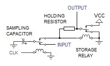
Instead of using a relay for the first latch, a capacitor is used to sample the INPUT signal by charging to VCC or discharging to ground. When CLK rises, the capacitor connects to the storage relay. If the capacitor was initially charged by the INPUT signal to VCC then it will dump enough current into the storage relay to cause it to actuate and then the holding resistor will maintain the state. If the capacitor was discharged by the INPUT signal to ground then it will suck away enough current from the holding resistor to cause the storage relay to deactivate. This design is also fairly robust and not very finicky because the holding resistor just has to be small enough of a resistance to maintain the relay actuation, and the capacitor size has to be large enough to store enough charge to change the relay state. Once you determine these two values, they work well across all relays with the same coil characteristics without tuning to each individual relay.
Digital Relay Circuits
I developed Catahoula Technologies Relay Logic Modules using the CMOS style method as basic building blocks for larger and more interesting relay based circuits. They could be used for fun educational purposes and somewhat resemble how modern solid-state digital design would be accomplished. The following sections are examples of various projects that could be built with these modules.
Binary Decoder
A RL4067 module could be used as a binary decoder as a great way to learn binary numbers and how it is decoded into individual one-hot outputs. This module is very similar in functionality to the solid-state CD4067 chip.
Conceptually, a binary number is treated the same way as a decimal number when it comes to incrementing, rolling over and carrying. The key difference is a binary number is base-2 with only 0 and 1 available while decimal is base-10 with digits 0-9 available. What do you do once you reach 9 and want to add one more? The first digit rolls over back to 0 and you perform a carry to the next decimal position to go from 9 to 10. Binary is the same way except the roll over and carry occurs when you're at the digit 1 and add one more to arrive to "10" or the equivalent of 2 in base-10. The decoder uses binary inputs to route a common signal through a relay based binary tree to an individual one-hot output. Using RL4067 and RL4100 modules, a self-contained demonstrator could be built using the following diagram.
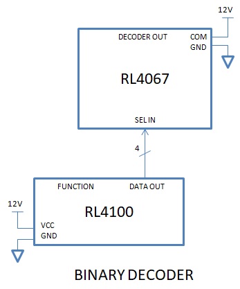
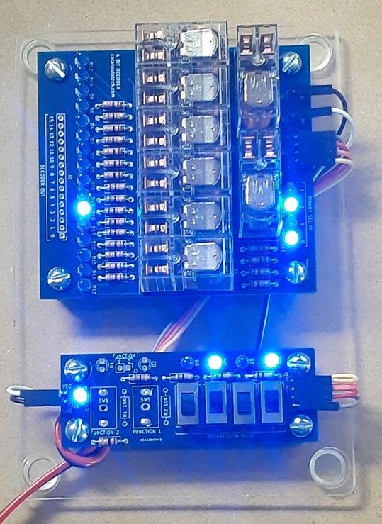
Here is what mine looks like assembled using an acrylic base with an input of 5 (b'0101') and a decoded output on the 6th LED (remember, an input of 0 will light up the 1st LED).
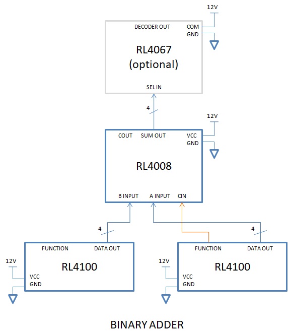
Binary Adder
A RL4008 module is equivalent to the solid-state CD4008 chip and is a 4-bit binary adder with carry input and output. This module could be cascaded to add larger bit widths. I built a simple 4-bit demonstrator with the RL4008 and two RL4100 modules using the following diagram.
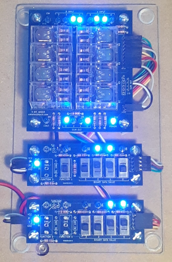
Here is what mine looks like assembled using an acrylic base showing the "A" value set to 6 (b'0110') and the "B" value set to 3 (b'0011') resulting in a SUM output of 9 (b'1001').
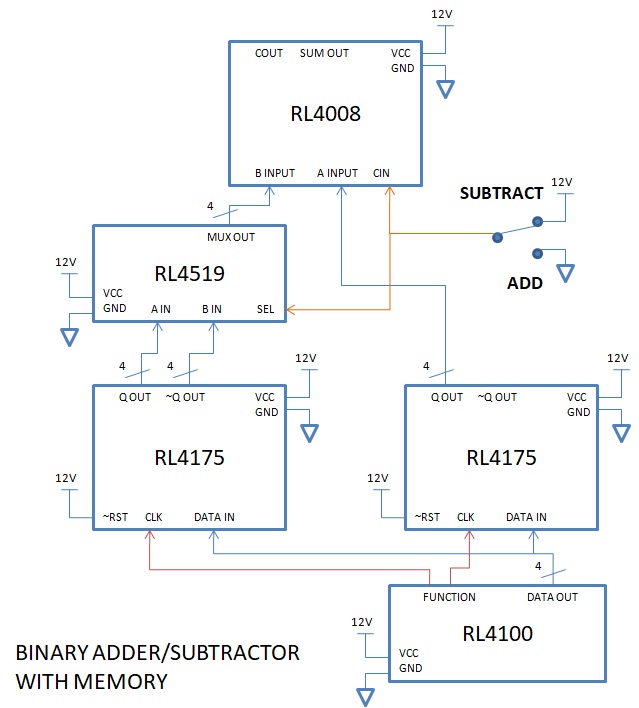
Basic Calculator (Binary Adder/Subtractor with Memory)
This is the Basic Relay Computer reinvented and similar to the "Homebuilt Computer" by Neil Ardley in the book "How Things Work." Again using the RL4008 module for a 4-bit binary adder, two RL4175 modules are used to store two values "A" and "B" from a single RL4100 control module. The output of the RL4175 modules are fed into the RL4008 to produce the sum of A and B. Two's complement subtraction is possible by doing a bitwise inversion of "B" and then adding 1. This is easily accomplished by wiring the inverted ~Q OUT of the "B" flip-flop output to the RL4008 to be added with "A" and feeding the carry input CIN of the RL4008 adder with 1 to perform the increment on the inverted "B". Effectively this makes the RL4008 perform the operation A minus B. The design could use a RL4519 quad 2-input mux to select between Q OUT and ~Q OUT of the "B" flip-flop depending on the switch setting to ADD or SUBTRACT as illustrated in the following diagram.
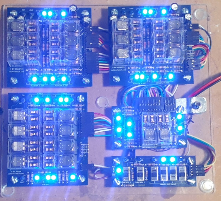
Here is what mine looks like assembled using an acrylic base with the "A" value set to 5 (b'0101') on the upper left register and the "B" value set to 6 (b'0110') on the upper right register and the SUM output is 11 (b'1011') on the lower left adder output.
Binary Counter
A binary counter is another basic use of the RL4175 D-type flip-flop module for sequential logic combined with a RL4108 binary incrementer module for combinational logic. The counter increments from 0 (b'0000') to 15 (b'1111') before rolling over. I built a simple 4-bit demonstrator with the RL4175 and RL4108 modules using the following diagram.
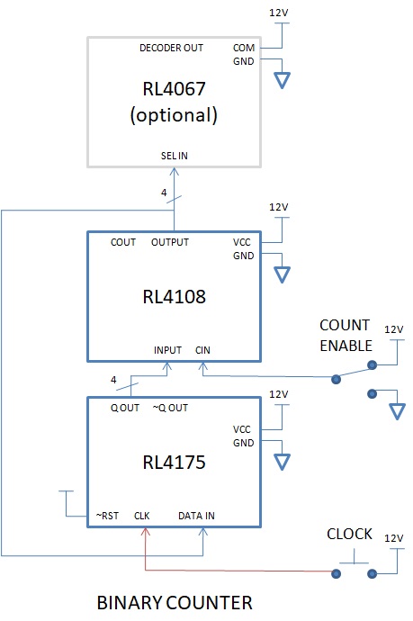
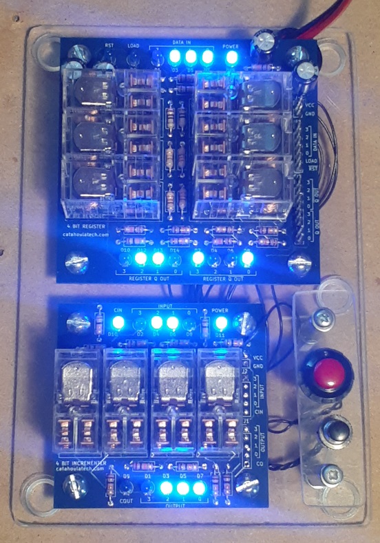
Here is what mine looks like assembled using an acrylic base showing the flip-flop output (Q OUT) = 6 (b'0110') and the incrementer output that feeds back into the flip-flop input (DATA IN) = 7 (b'0111'):
4-digit Binary or Nixie Clock
Now things become more interesting. A 12-hour four digit nixie clock can be assembled from the relay modules. The following diagram shows a fully synchronous clock design in which all D-type flip-flops use the same 1 pulse per minute (PPM) clock source. Most DIY digital clock circuits out there including many of my solid-state designs on this website will use an asynchronous chain of counters. A 1 minute counter would reset itself after counting 0 to 9, and advance the 10 minute counter shortly thereafter by pulsing its clock. This yields a very simple circuit, but it's generally scorned upon in the industry nowadays because it is more difficult to perform setup/hold timing analysis. However, while these solid-state asynchronous counter chains might happen to work, the relay modules usually reveal the potential timing failures of asynchronous digital designs because relays are extremely slow compared to solid-state circuits. So, below is a digital clock design using completely synchronous digital logic that follows current industry "best practices" except for using relays as digital logic, of course.
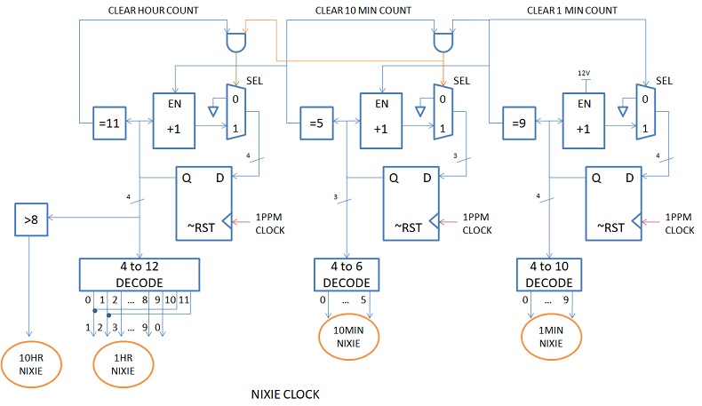
The diagram is more simplified and does not show the exact usage of relay modules. Here is a guide:
- DECODE blocks use RL4067 partially populated with relays as needed by the size of the decoder. There is no need to populate all 8 relays if not all input or output bits are used. The COM pin is tied to ground for the nixie cathodes and the decoder output LEDS should NOT be populated.
- +1 blocks use RL4108 with its CIN bit being used as the "EN" enable signal so when CIN=0, the incrementer does nothing and passes the input to the output.
- D-type flip-flop blocks use RL4175 with ~RST connected to 12V and all modules are clocked by the same 1 pulse per minute 12V clock source.
- =5, =9, =11 blocks are combinational logic to detect when the binary value equals those values. "=5" outputs true when the binary value bit 2 and 0 are true (b'101), "=9" outputs true when the binary value bit 3 and 0 are true (b'1001'), and "=11" outputs true when the binary value bit 3, 1 and 0 are all true (b'1011'). All of these can be accomplished using AND gates in the RL4079 module.
- Select 0 or 1 mux use RL4519 to select between the increment "+1" output or all zero to clear the counter.
- >8 block is combinational logic that outputs true when the binary value is greater than 8 so the 10 hour nixie lights up a "1" when the binary value is b'1001 (10), b'1010 (11) or b'1011' (12). This can be done using an AND gate between bit 3 and the output of a OR of bits 1 and 0 using the RL4079 module.
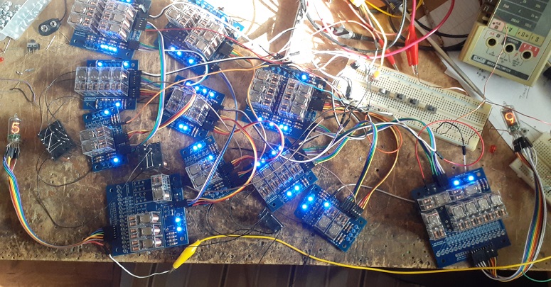
Picture of the unfinished assembly in progress showing the functional minutes nixies at "59" (5/30/2021):
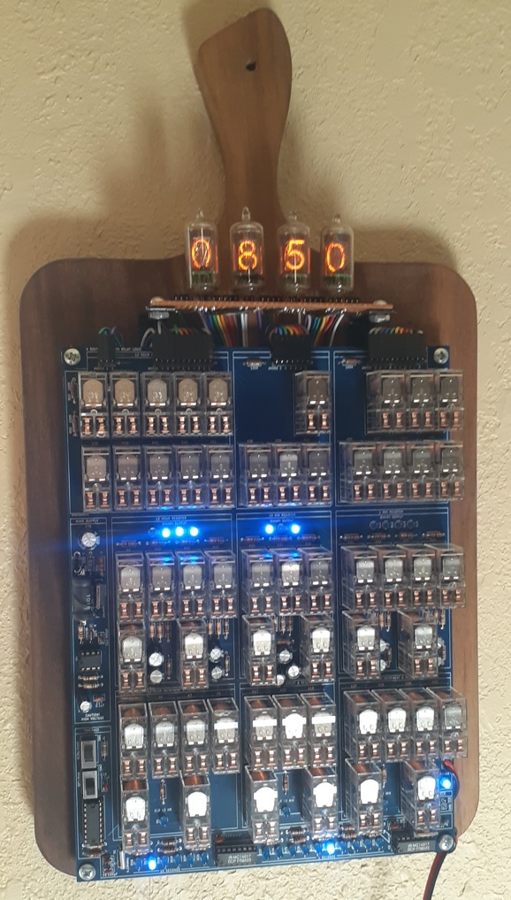
After building a successful prototype of the 4 digit nixie clock using relay modules, the entire design was put on a single board with some optimizations and uses 55 Omron G2R-2 12VDC DPDT relays. Here is a video of the single board version in operation. The newer revision of the board only requires 54 relays as a relay in the 1 min decoder was not necessary.
Board datasheet: RL1200_ds.pdf
Schematic: RL1200_sch.pdf
I mounted the board and nixies on a 8x12" wooden cutting board and hung it up on the wall. Here is a photo and another video of the finished project.
Interested in building relay logic circuits? Consider buying Catahoula Technologies Relay Logic Modules and Catahoula Technologies 4-digit 12-hour relay nixie clock.
Back to Top