Analog Oscilloscope Pong
Return to Home
Return to Projects
Version 1: Traditional Pong
Pong is a very simple game that could be done using analog circuits. In fact, analog circuits have been used for creating Pong games on the television. The Magnavox Odyssey is one example of a commercial game console using analog circuitry and my Analog TV Pong Game for the TV is a homebrew example. Vector graphics depend on voltage levels rather than timing pulses, so a common approach for generating XY graphics for an oscilloscope is to use a digital-analog converter (DAC). The DAC converts the digital outputs from a microprocessor to analog voltage levels. However, this analog pong game circuit was built to show that a pong game with such simple graphics could be done using discrete components.
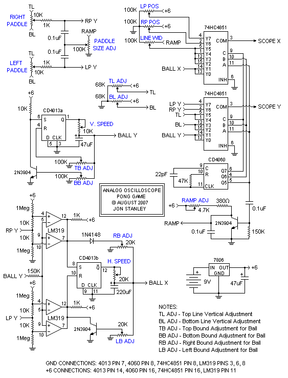
Six chips was used for a single/two player pong game; four chips are simple 74HC-series or 4000-series and the last two are dual operational amplifiers. However, there are 13 potentiometers (excluding the paddle controllers) for various adjustments in this delicate analog circuit and a general alignment instruction is listed below in this webpage. Below is the schematic of the analog pong game that generates XY vectors for an oscilloscope.
It is simple to be complicated, but complicated to be simple. While the circuit may appear relatively simple, the alignments can be rather tricky. Below are general alignment procedures:
- Set all pots to the medium range then apply power. The 4013 most likely will oscillate or stick, but ignore this for now. With the oscilloscope in normal operation, probe RAMP output and adjust the 4.7K resistor until the wave appears like a ramp/triangle waveform with the largest amplitude possible.
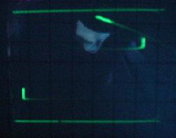
- Connect the X and Y output of the circuit to the respective oscilloscope X and Y inputs, and then try to center a picture. Note that the input amplifiers will have to be cranked up (my oscilloscope was set at 0.5V per division for the vertical and 0.2V per division for the horizontal). Try to locate the ball in the picture.
- Adjust TB ADJ and BB ADJ away from ground to get the ball to bounce up and down. V. SPEED may need to be adjusted for the bounces to start because the TB ADJ and BB ADJ pots bleed away some of the capacitor’s charge for the BALL Y signal. If it is too difficult to start the bounces then disconnect pin 4 and hook up a 10K pulldown resistor to ground. Take a wire from +6 and tap pin 4 and see if the ball rises and bounces back down. If the ball is already up, then adjust TB ADJ until the ball starts to bounce down. When this is achieved, reconnect pin 4 to the original circuit and adjust BB ADJ until the ball goes up and down with the largest up/down deflection.
- Adjust TL ADJ and BL ADJ until the top and bottom lines match the maximum and minimum vertical positions of the ball while it is bouncing up and down.
- Adjust RB ADJ and LB ADJ away from ground until the ball starts moving horizontally and bouncing back and forth. H. SPEED may need to be adjusted. Refer to step 3 if starting the bounce is too difficult, but instead of disconnecting pin 4, disconnect pin 10.
- Adjust LINE WID until the width of the top and bottom lines extend nearly to the point where the ball rebounds horizontally. Adjusting RAMP ADJ can move the lines horizontally if necessary.
- Adjust LP POS and RP POS to place the paddles at the points where the ball bounces off when it hits the paddle. Adjusting the paddle until the ball hits the paddles directly will be necessary. The goal is to get the ball to bounce right off the paddles, but if it misses, it goes beyond the paddles slightly then rebounds. Readjusting RB ADJ and LB ADJ may be necessary.
- Adjust PADDLE SIZE ADJ for the preferred paddle size. V. SPEED and H. SPEED can be adjusted to vary the ball speed, but if there is too much resistance then the ball may not bounce due to reasons explained in step 3.
How it Works
The game graphics works largely because of the 74HC4851 eight-channel analog switches. The 4060 is a clock chip with a frequency set by the 22pF and 47K resistor and outputs binary pulses that are used to multiplex the input channels of the 74HC4851 to output single X and Y signals from the various input signals. The ball signals are fed in both Y0 and Y1 to extend the drawing cycle so the dot appears brighter. The top and bottom line signals are fed in two channels as well to make the lines brighter. Each paddle signal is only fed into one channel of the 74HC4851.
The RAMP signal is generated by the charging action of the 0.1uF capacitor, which is discharged by the pulses from the 4060. Note that the transistor is activated every time there is a pulse on pin 5. When the first bit of the 74HC4851 goes high, the capacitor discharges so the RAMP signal is synchronized with the top and bottom lines and the paddles.
The paddle signals LP Y (left paddle Y) and RP Y (right paddle Y) are generated simply by varying the voltage level on the Y-axis with a pot. The maximum and minimum points for the paddle are generated by the voltage level of the top line (TL ADJ) and bottom line (BL ADJ) positions. Moreover, to give the paddles their length, the Y signal voltage is injected with some of the RAMP signal. The size is adjusted via the PADDLE SIZE ADJ.
The ball Y position is generated by a very simple flip-flop that charges or discharges a RC network. CMOS has nice high impedance inputs, so when the capacitor charges up to the minimum threshold to be interpreted as a logic 1, it can be used to set or reset the flip-flop. The top bound adjustment (TB ADJ) adjusts the RESET threshold level so the capacitor has to charge up to a certain voltage level before it triggers the RESET. When the flip-flop changes state and discharges the capacitor, the bottom bound adjustment (BB ADJ) is adjusted so the NPN transistor stays activated when the capacitor is above a certain minimum voltage level. When the capacitor discharges below this minimum threshold level, the transistor deactivates and SET will be pulled up to +6V via the 10K resistor. The BALL Y signal is simply the voltage level on the capacitor.
The flip-flop for the ball X position works very much like the one for ball Y, but with an important difference. LM319 dual operational amplifiers (op-amps) are used as a window comparator to detect when the ball Y position matches the paddle Y position. When ball Y is within the "window" of the paddle signal, both op-amps outputs are pulled up to +6V by the 1K resistor. However, the ball should only bounce off the paddles, so the right bound adjustment (RB ADJ) and left bound adjustment (LB ADJ) are used to prevent the op-amps from setting or resetting the flip-flop until the ball X signal is at the paddle’s X position. Note that the op-amp outputs, diode or transistor, and the 1K resistor all create a simple 3-input AND gate. It is important to note that if the ball misses the paddle due to the ball Y not matching the paddle Y signal, it will continue off the playfield slightly until the Y signals match to send it back the other direction.
If one prefers to have a circuit to stop the ball from rebounding into the playfield after it misses the paddle, then using an extra dual op-amp can be used as a simple comparator by sensing when the ball X position is beyond the paddle position to pull down the S or R inputs, thereby preventing the possibility of a rebound until the output of the op-amp is disconnected, perhaps via normally closed (NC) pushbuttons. This idea basically turns the 3-input AND into a 4-input AND for this condition.
The game is not really challenging because the ball does not change angle or speed when it hits the paddle in certain ways. The ball simply reverses horizontal direction when it hits the paddle. Moreover, if V. SPEED and H. SPEED are adjusted so the ball moves slowly, one can notice how it follows the capacitor charge/discharge curve rather than a linear path. Using op-amps for triangle wave generators instead of the 4013 flip-flops might be a better option but not explored in this project. The game simply demonstrates how simple parts can be put together to make a game without using a microprocessor. The project cost me nothing; all the pots were taken off dead computer monitor boards and I had extra chips from previous projects.
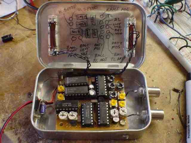

The circuit was stuffed on a small 2" x 3" PCB and fitted in a painted Altoids tin.
Version 2: Round Pong
Simple discrete circuitry to generate a Pong game with a round playfield is not impossible. Microcontrollers make things too easy so I challenged myself to make a playable round pong game using discrete analog components and basic digital flip-flops. After a year of working on a design during my spare time, lo and behold, I came up with a working design using components I had on hand. Below is a schematic for Round Pong:
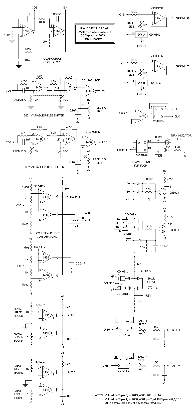
The design uses ten 1458 dual op-amp chips, two CD4013 dual D-type flip-flops, one CD4081 quad AND gate, and one CD4066 quad analog switch. The grand total of chips used in this design is 14, but some op-amps come in packages of 4 so the IC count could be trimmed down to 9. Note that all the diodes are IN4148.
The circuit requires a dual rail power supply that produces +5 and -5 volts and is not shown in the schematic. One of the main reasons for using the 4000-series CMOS logic is because they can run on a wide range of voltages up to around 15V. Because the analog circuitry operates on a range of voltages between +5V and -5V, the ground connection of all CMOS chips are connected to -5 and Vcc to +5. As a result, -5V is LOW (logic 0) and +5V is HIGH for the digital components in the design, unlike traditional TTL in which 0V represents LOW and +5V is HIGH. Lastly, the design presents a great collection of various op-amp circuit topologies.
How it Works
Below is a pretty thorough and intensive explanation of the circuit design. The documentation is also for my own benefit because I do not always remember my reasoning behind certain design choices if I don't write them down. Hopefully you can find the documentation to be educational, but if not then skip ahead to the pictures.
The Round Pong game is designed around a circle generator. There are a number of ways to achieve a circle generator and the easiest with op-amps is a typical Quadrature Oscillator circuit shown in the upper left of the schematic. The oscillator consists of two op-amp integrators. By assuming the input is a sine wave, the output after two integrals of the sine is a negative sine. Consequently, the sine wave experiences a 180-degree phase shift that is a recipe for oscillation. The 100K resistor and 0.01uF capacitor sets the oscillation frequency to about 160Hz. Each op-amp output will produce a sinusoid signal that is 90-degrees out of phase with each other (quadrature) and are labeled SIN and COS.
Feeding SIN into the X and COS into Y, or vice versa will produce a circle on the oscilloscope screen. If you are familar with Lissajous figures then recall that X and Y sinusoid signals with the same frequency will produce a diagonal line with slope 1 on the screen with zero phase shift. A circle represents 90-degree phase shift, and a diagonal line with slope -1 represents 180-degree phase shift.
We can draw a circle with the quadrature oscillator and a XY scope. By changing the amplitude of SIN and COS, the circle size can be adjusted. To draw paddles, the SIN and COS signals can be chopped up to draw an arc where a paddle will be located. There are many methods for drawing a paddle.
One of my early ideas was to take a reference point on a circle, mainly by generating a square wave that is synchronized to the SIN signal and create a pulse that has variable delay with respect to the rising edge of the square wave. Delay is easily achieved with digital timers, shift registers, or counters. This also allows the use of a "spinner" paddle control that would use a mouse ball wheel sensor to operate a 4-bit up/down counter. By using a CD4060 clock counter chip that produced binary counts that were synchronized to the circle and each count represented one of 16 "pie" slices of the circle, the counts are compared to the up/down counter from the paddle. When the two counts were equal, the circle is switched through to the oscilloscope to draw an arc that represented the paddle. There are two major drawbacks to the digital approach. First, the paddle can only be located in one of 16 pie slice locations and paddle movements were simply jumps between slices of the circle. Second, the design would have used about 3 or 4 relatively sophisticated digital chips per player, including a 4-bit up/down counter and a 4-bit comparator.
The solution shown in the schematic above uses a 360-degree variable phase shifter. Observe that there are two cascades that are identical. Each cascade is basically an all-pass filter with variable phase shift up to 180 degrees. Two cascades can yield up to 360 degrees of phase shift, with one minor downside being the use of a dual-gang potentiometer to vary the phase of both cascades simultaneously so one potentiometer can vary the shift between 0 and 360 degrees. Finally, the phase-shifted output sinusoid is sent through a level comparator. When the sinusoid voltage is greater than the voltage on the - input of the op-amp comparator, the output is +5V (HIGH), otherwise the comparator outputs -5V (LOW). The voltage on the - input of the comparator can be adjusted with a potentiometer aptly labeled "Paddle Size" because it will adjust the size of the pulse output from the comparator depending on the voltage levels of the sinusoid that are to be interpreted as a logic HIGH. I think the phase shift method is the easiest way of producing a variable delayed pulse by varying the phase of the sinuosid and later converting it into a pulse with analog circuitry than to try delaying the pulse itself. The outputs Aon and Bon represents the timing when a paddle arc should be drawn, i.e. +5V means draw a paddle and -5V means don't draw a paddle.
Now to address the timing issues that was quietly ignored two paragraphs back, consider when paddle Aon or Bon is HIGH and the scope draws an arc. What happens when Aon or Bon is LOW? Turning off the circle generator to the scope results in a dot in the center of the screen, which is not desirable especially for collision detection. So I designed the timing to draw a ball all the time, and only take a slice out of the ball to draw the paddle when Aon or Bon was HIGH. The result worked great except the ball was sliced out, so by alternating between two display modes, the ball was drawn completely in one cycle and then in the next cycle the ball was sliced out to draw the paddle. The result was a clean drawing of the paddles and ball without any dead elements appearing on the screen.
The two circuits at the upper right of the schematic are where the paddle and ball signals are generated. The op-amps are wired as unity gain voltage followers so they serve to buffer the signals for the oscilloscope. The CD4066 switch is used to connect the BALL SIZE pot to the BALL position voltage. There are several nice tricks accomplished with this simple circuit. First, when SW A or SW B is off, no current flows through the 100K resistor and the size pot, so the voltage that appears to the scope is almost identical to the COS or SIN signal. As a result, the scope draws the circle in its full size. When SW A and B turns on, BALL X and Y are slow varying DC values that appears like AC shorts. As a result, the AC signals SIN and COS are attenuated by the voltage divider effect resulting from the 100K and the SIZE pots, so the circle on the screen is now smaller. The second effect is the BALL X and Y values create a DC offset on the input of the op-amp buffer so the smaller circle now offsets to a X and Y position based on the voltage levels of BALL X and Y.
By tracing the signal T back to a 2N3904 circuit, the logic function is T = ((Aon+Bon)*CLK)'. In other words, when either paddle A or B should be drawn, and the display mode (CLK) allows the paddles to be drawn, then T is LOW. When SW A and B (CD4066 chip) sees a LOW control signal then it turns off and the SIN/COS signals go to full size to draw the paddle. When T goes back HIGH then SW A and B turn on to attenuate SIN/COS back to ball size and adds the BALL X and Y offset. The logic function for T can be realized with a very simple combination of diodes, resistors, and a transistor. The idea is when Aon or Bon are HIGH (+5V) then current flows through one or both diodes and through the 47K resistor to the base of the transistor. If CLK is HIGH then the third diode is reverse biased and current can flow through the base of the transistor to turn it on. As a result, T is pulled down LOW to -5V. If CLK is LOW then the diode draws current away from the transistor base and results in the transistor turning off so T is pulled up HIGH. The 0.1uF cap across the 47K supresses high frequency oscillation. Due to the delicate balance of generating and drawing away currents, this circuit is not very easy to get up and running reliably so the 47K resistor and 0.1uF cap may need tweaking.
CLK and CLK' are produced by a CD4013 flip-flop that divides the COS frequency by 2. In other words, CLK changes logic state every time COS makes one complete cycle. The COS signal is converted to a square wave with another level comparator with the comparsion voltage set to 0V so the duty cycle of the square wave is roughly 50%.
Now everything that has been explained up to now was the easy part. Collision detection is difficult when the paddles are allowed to move in a two-dimensional manner on a circular path unlike Version 1 in which the paddles were constrained to one-dimensional vertical motion.
Taking cue from Version 1, window comparators are used to compare the ball to the paddle. The difficult problem is that the ball and paddle signals are not generated simultaneously. However, the paddle is simply a slice of the full size circle created by SIN and COS so we compare SIN and COS to the ball signal seen on SCOPE X and Y at the correct times. SCOPE X and Y will produce a complete ball when CLK' is HIGH, which is the drawing cycle time when the ball is drawn completely without slices out of it for the paddle. We want to compare the ball X and Y signals to SIN and COS only during the times when SIN and COS actually represent the paddle. So the logic function for determining the timing when to compare the signals is PL = ((Aon + Bon)*CLK')'. Notice that PL is identical to T except it is produced during the ball drawing mode rather than paddle drawing mode. Furthermore, for the game to track turns, Aon and Bon are combined with TURN and TURN' via AND gates so the actual logic function is PL = ((Aon*TURN + Bon*TURN')CLK')'. On one last note, this circuit is not easy to get up and running and the 220K resistor may need tweaking. In the final perfboard version, a parallel 47K resistor and 0.1uF capacitor combination on the base of the transistor fixed some issues with the ball "leaking" through the paddles. The 0.1uF cap is used for supressing high frequency noise resulting from the diode logics, and the 47K serves as a bleeder to prevent the 0.1uF cap from charging up completely.
When the time is right to compare SIN and COS to SCOPE X and Y to determine if the paddle collides with the ball, PL goes LOW which turns off SW C. As a result, if there is collision then all the 1458 window comparator op-amps will go HIGH and BOUNCE is pulled up HIGH due to the 10K resistor. A 0.001uF capacitor is used to smoothen the BOUNCE signal for other logics. In retrospect, I think when I named the signal PL it means Paddle Low, because the signal is LOW when SIN/COS represents a paddle.
The problem of collision detection is not entirely solved yet because there is no way to distinguish the kind of bounce that should commence based on the paddle angle and ball movement. Refer to the figure below for two basic types of bounces:
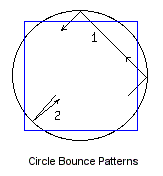
Notice that there is a blue square over the paddle circle path to represent the boundaries for when a bounce should reverse in horizontal, vertical, or both directions. This hints at exactly what kind of window comparator we need to determine X and Y reversal. The two window comparators at the lower right of the schematic shows four potentiometers that adjust the 4 boundaries that make up the blue square in the figure above. The labels may be a bit misleading, but I shall explain. Vertical right and left bounds reflect the horizontal boundary locations that the ball must be within for BALL Y to reverse when collision results. Likewise, horizontal upper and lower bound reflect the vertical boundary locations that the ball must be within for BALL X to reverse when collision results. If the ball is within all four boundaries upon collision then it is evidently at one of the four small corner areas that would result in both BALL X and Y reversing for a diagonal bounce. This serves as a rough approximation of how a ball would ideally bounce off a curved paddle.
The signals XR and YR produced by the boundary detection circuitry are combined with BOUNCE to produce a signal that will change the BALL X or Y directions respectively. BALL X and Y is produced by a CD4013 with two flip-flops charging or discharging a large capacitor. Although the capacitor charge/discharge response is nonlinear, it is reasonably good enough for a simple game. The flip-flops are wired with the inverting output looped back to the data input, so every time the flip-flop is clocked, it will change state. Basically, these flip-flops are wired to act like a Toggle flip flop. If the player misses and the ball goes out of the playfield, then XREV and YREV can be overridden via the BALL SERVE pushbutton.
When the BALL SERVE pushbutton is pressed, the flip-flops change state and the ball returns to the playfield. The Player Turn Flip-Flop keeps track of which player has the turn to hit the ball and the turn outputs are readable through LED indicators.
Notes on gameplay
- The paddles are controlled by a dual-gang pot and the movement is nonlinear, i.e. turning the pot will move the paddle slowly then suddenly very quickly, or vice versa. Also the pot is limited in rotation so the paddle has to be controlled back and forth to get it to the desired position.
- Ball X/Y size and Ball X/Y speed can be a dual-gang pot for easy control of size and speed.
- If a player has a turn and misses the ball then the ball goes out of the circular playfield and can only be returned to play via the BALL SERVE pushbutton. The player who misses the ball will continue to have the turn to hit the ball, but the turn flip-flop can occasionally be tricked in giving the turn to the other player.
- The paddle size can be adjusted to maximum size, which is a full circle. The ball will perpetually bounce around inside the circle.
- One can bypass the turn tracking by disconnecting the AND gates that combine Aon, Bon with TURN and TURN' and wiring Aon and Bon directly to the diodes. The ball will bounce off either player regardless of which player has the turn. This allows for single player play by adjusting the second player to have a C-shaped circle and the main player has a small paddle to try and keep the ball from leaving the opening in the C.
- The only alignments required in the game are the bounds. To begin, set all the bound pots as close to their 5V or GND terminals, and set both paddle sizes to max so the ball bounces inside the larger circle. The ball should bounce diagonally. Slowly adjust one of the four pots until the ball starts to bounce in one dimension rather than two (i.e. X or Y reverses, not both) on the boundary area under adjustment. Repeat for all remaining pots. If the ball "leaks" through the larger paddle circle then back off all four pots a bit closer to their 5V or GND terminals and fiddle from there until no "leaking" occurs.
- A bounce sound could be added to the game by using the BOUNCE signal to trigger the sound generation circuitry, or take advantage of the change in state of TURN and TURN'.
Final Product
My original intent for this game was to repurpose an old round CRT oscilloscope. The ball will not be visible when it goes out of the circular boundary. All the oscilloscope function knobs on the front panel will be removed and rewired to various controls in the game, including the two player paddles, paddle size, ball X and Y size and speed. I also added sound to the bounces using the following circuit:
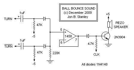
The circuit makes use of the last remaining unused op-amp in the original round pong circuit. The 1uF capacitor and 47K resistor combination will generate a brief pulse whenever the TURN and TURN' signals change state. The diodes and 220K resistor act like an OR gate to react to a rising edge on TURN or TURN'. The op-amp buffers this logic signal and outputs a pulse that is long enough for a short but audible sound whenever the BOUNCE signal triggers the turn flip-flop to change state. This part of the circuit serves as a quick and dirty one-shot monostable on TURN and TURN'.
The CLK signal runs at around 160 to 200Hz. Using CLK to drive the piezo speaker will generate a low frequency beep. When the op-amp output is low (-5V) then the diode pulls down the base of the transistor so no sound is generated. When the turn flip-flop changes state and causes the op-amp to output high (+5V) for a short time, the diode is reverse biased and CLK is allowed to pass through to generate the beep briefly.
I built the final version of the round pong game in a 50s Heathkit oscilloscope that contained the guts of a later 60s solid-state Heathkit. Pictures and video are shown below.
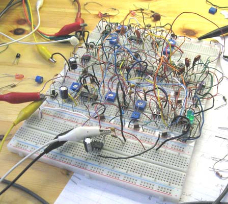
The entire game circuitry on a breadboard. Lovely forest of wires.
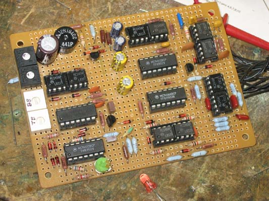
The final circuit on a perfboard.
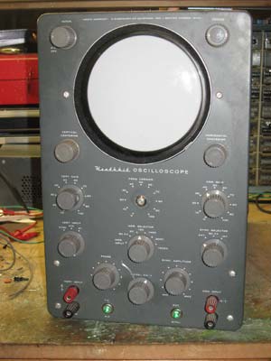
The donor oscilloscope. Notice the two green LEDs at the bottom for indicating player turn. The middle column of knobs are for ball speed and size, while the adjacent columns of knobs are for player paddle A and B control. The upper 6 knobs are for the oscilloscope, including horizontal and vertical size and centering.
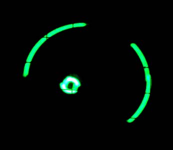
The paddle size was adjusted to clearly show the arc in the picture.
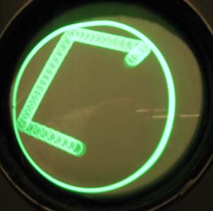
A 2.5 second exposure of the game with the paddle size at maximum.
Back to Top