The Tektronix 4052 System
Return to Home
Return to Resources

The Story
In late 2004, an electrical engineer friend of mine who had worked for Tektronix from 1973 to 1983 was clearing out his garage and invited me over to look through a pile of equipment he was planning to toss. When I arrived, I discovered that the pile was mostly Tektronix-branded gear, and among it was a 4052 computer. At the time, I only knew Tektronix for their high-end oscilloscopes and test equipment, so I was surprised to learn they had ventured into the computer market at the time. My friend told me he thought the stuff was good for parts, but I decided to rescue the 4052 along with a few related peripherals. Unfortunately, the 4052 did not function properly when I powered it up. It appeared to go through the correct startup sequence judging by the front panel indicators but the screen remained blank. I fiddled with the brightness and bias controls on the display board but could only produce a static dot on the screen.
Regardless, I kept the 4052 and left it sitting for about a year. Then I get a call again from my friend that he was cleaning out more of his stash and gave me another 4052. This second unit was barely functional; it would power up, and if I was lucky, a cursor might flash briefly. Between the two machines, I could swap boards with the hopes of getting a functional computer out of the two. I also found two sets of preprogrammed Tektronix BASIC interpreter ROMs from him. After installing the ROMs into one of the 4052s and doing some board-swapping, I finally got a system to function enough to play with. It was an exciting early foray into retrocomputing for me as I was 16 years old at the time. My earliest memory of using computers growing up were IBM PC-compatibles from the late 1980s to 1990s running MS-DOS or Windows 3.1, so using a computer from the 1970s or early 1980s was an entirely new experience. At the time, I had no way of loading or storing programs on the Tektronix 4052 so every time the computer was powered up, I would manually type in simple programs in Tektronix BASIC to run a short demo.
Fast-forward to the 2020's, a small community of Tektronix 405x enthusiasts and the Vintage Tek museum had invested significant time in documenting and sharing technical information to make the most out of the 405x computing experience. I came across far more resources available online than when I first tinkered with the 4052 in the mid-2000's.
Useful links:
- Tektronix 4050 - Wikipedia
- Tek 4052 wiki - w410.com
- Vintage Tek 405x Museum Page
- 405x Program Archives - VCF Forum thread and repository of recovered tapes and programs, and some new programs
- 4052 firmware - Bitsavers.org archive of 4052 ROM dumps and diagnostic pack ROM
- 4052-54 diagnostic ROM pack
- 4052 Multifunction ROM Module (MFM)
- Tek Vectors YouTube channel - Monty McGraw's videos of his 4052 and 4054 in action
The Tektronix 4050-series Systems
The Tektronix 4050-series systems were produced by Tektronix, Inc. based in Beaverton, Oregon in the late 1970s and into the early 1980s. When I originally searched on the Internet for "Tektronix 4052" in early 2005, the there was scant information about its history and specifications so I had to do old-fashioned information gathering from former Tektronix employees or past users of these systems. Below is a high level summary of each 405x model from what I had gathered at the time:
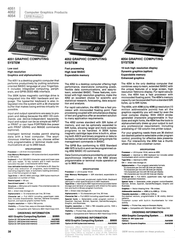
- 4051 was a 8-bit 6800 processor-based system introduced in 1975 for the base price of $5995 with 8KB RAM. The RAM was expandable up to 32KB for an additional $1900. The 6800 processor had a top speed of 1MHz at the time. The display was 11" with 1024x768 pixel resolution.
- 4052 was a vastly improved version of the 4051 using four bit-slice AMD 2901 processors operating on 16-bit wide data and was engineered by Tektronix to be backwards compatible with 6800 programs and could run significantly faster than the 4051. Tektronix inserted custom instructions to the 6800 instruction set so the 4052 could do floating point computations about 30x faster than the 4051. The 4052 was introduced to the market in 1978. The cost for the base unit with 32KB RAM was $9800, expandable to 64KB for an extra $2000.
- 4054 was a much larger version of the 4052 a 19" display and 4096x3072 pixel resolution. This graphics capability was unheard of in the late 1970s and the reason these systems were used for high resolution graphics work. The 4054 used the same bit-slice processor design as the 4052. The base unit cost $16500 with 32KB RAM, expandable to 64KB for an extra $2000.
The 4050-series computers were all equipped with a 3M DC300 tape drive for loading and storing programs. They supported IEEE-488 (GPIB) to enable interfacing to a wide variety of electronic equipment available. The IEEE-488 standard, originally developed by Hewlett-Packard in the late 1960s as the HP-IB (Hewlett-Packard Interface Bus), was designed to simplify communication between test instruments and controllers in automated measurement systems. Recognizing its utility, the Institute of Electrical and Electronics Engineers formalized it in 1975 as IEEE-488, later refining it into IEEE-488.1 and IEEE-488.2 to address protocol and compatibility issues. Its robust parallel architecture allowed up to 15 devices to communicate over a single bus, making it ideal for laboratory and industrial environments. Throughout the 1970s and 1980s, IEEE-488 - also known as GPIB (General Purpose Interface Bus) - became the de facto standard for connecting oscilloscopes, multimeters, signal generators, and early computers, with widespread adoption by manufacturers like Tektronix, HP, and National Instruments.
Tektronix provided a complete ecosystem of 405x software libraries, electronic instruments and periperhals to use with the 4050-series computers. As a result, Tektronix had success selling to university labs, industry and government in the late 1970s to early 1980s. 4050-series supported peripherals included:
- Storage Devices
- Tektronix 4924: External DC300 tape drive (same format as internal 4050-series drive)
- Tektronix 4907: File Manager (8-inch floppy disk system using Shugart 851R drives)
- Printers and Plotters
- Tektronix 4641: dot-matrix 132-character line printer
- Tektronix 4642: dot-matrix 80-character line printer
- Tektronix 4631: hard copy unit (thermal printer)
- Tektronix 4662: single-pen XY plotter (or 8-pen Option 31)
- Tektronix 4663: large XY plotter
- 1981 Plotter brochure - dvq.com
- Input Devices
- Tektronix 4952: joystick for display cursor control
- Tektronix 4956: digitizing graphic tablet

A copy of the original 1980 brochure of the entire 4050-series and peripherals can be found here on dvq.com.
The Tektronix 4052
Display
The 4052 is unique compared to other computers of the late 1970s because of its vector-based display and the DVST (Direct View Storage Tube). Tektronix was in the unique position of being a leader in oscilloscope technology and the DVST was their method of capturing oscilloscope single-sweep waveforms on a screen for examination. The DVST was developed by Tektronix in the late fifties and contains a special plate over the CRT face that continuously glows when the electrons emit off the phosphor of the CRT face. At the time most computers had to implement video memory to store pixels and characters to display information. RAM was very expensive at the time so video memory was limited and consequently display resolutions were low. Tektronix likely saw the DVST as a competitive advantage in the fledging computer market because it eliminated the need for video memory and unburdened the processor from performing video related operations. The DVST itself was literally the "analog" video memory for displaying information. The 405x series uses what is called a vector-based display in which the processor simply moves the CRT beam from a specified point to another on the screen in a manner very much like an Etch-a-Sketch. Vector displays do not require pixel information to be written to video memory and then rasterized out like what the majority of computers did. When the 4052 starts up, it uses the Cartesian plane coordinate system with the X axis at 0 to 130 and the Y axis at 0 to 100 for defining the coordinates for which all BASIC commands can position the cursor and draw lines. This window actually could be changed with a simple command in BASIC. One other distinction with the DVST screen is that the computer only has to draw its graphics once and the screen stores the line. The Vectrex game system is another example of a vector-based display, however, it uses a conventional CRT and has to repeatedly draw out the graphics for the same reason a raster display has to repeatedly scan the screen because the CRT phosphor illuminates temporarily. The repetitive refresh rate causes flicker, but the DVST does not have flicker.
However, there is a downside to the DVST. Whatever is drawn literally remains including text! If you made a mistake in your typing, backspace only goes back one space, but it doesn't actually clear anything on the screen. Your option was either to press RUBOUT to blotch out that bad character and then resume typing, or hit the HOME/PAGE key to trigger the DVST to flash bright green to completely wipe the screen and then have the computer start over redrawing all the text. The blinking cursor is not stored on the DVST because it uses "write-through mode" that lowered the brightness of the beam low enough to activate the screen phosophor to be visible, the secondary electron emissions off the CRT face was insufficient to activate the DVST. The biggest limitation of the DVST is that it greatly limited the type of interactivity and animated graphics that we have come to expect on any computer because it doesn't have the rapid refresh capability of raster based displays. The HOME/PAGE erase takes about 1 second to complete. The only kind of animations that could be possible would have to take in consideration that whatever is drawn remains and games that have been developed for these machines include things like Lunar Lander. These computers were aimed towards higher end markets that needed high resolution graphics for CAD (computer-aided design) visualization and were not catering to those who wanted higher levels of graphics interactivity and games.
Hardware
The 4052 has a large motherboard assembly that consists of four individual boards: ALU (Arithmetic Logic Unit), MCP (Memory Control Processor), MAS (Memory Access Sequencer), and the I/O (Input/Output) boards. Below are pictures of the motherboard top and bottom views.
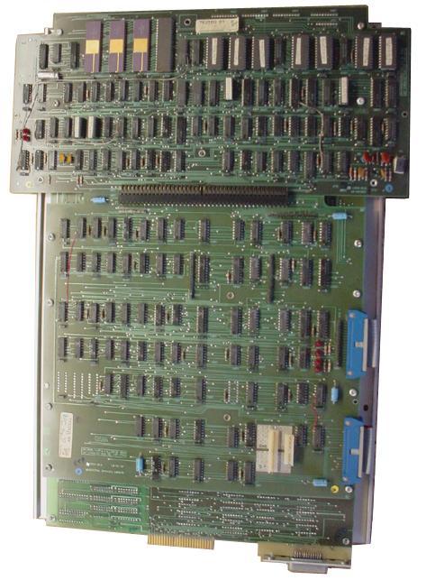
The top of the motherboard assembly are two boards, the top board in the photo is the ALU which contains the four bit-slice 2901 processors and microcode ROMs. The MCP board is at the bottom of the photo. The 5V power supply feeds into the MCP board on the left of the ribbon cable.
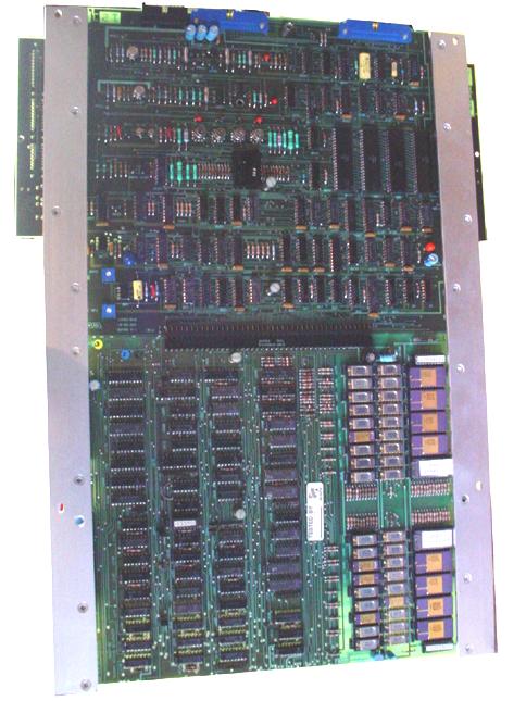
The bottom of the photo is the MAS board, which contains the 8 BASIC interpreter ROMs, 4116 dynamic RAMs (DRAMs) and the IEEE-488 GPIB port. At the top of the photo is the I/O board, which contains several D/A (Digital/Analog) converters to convert the digital signals into analog X and Y signals for the display. The I/O board also receives the keyboard input, tape drive signals, and other power sources besides 5V. Below are views of the 4052 with the cover removed.


Below is a view of the rear with the Option 3 4-slot backpack for feature expansion ROMs and has a built-in RS232 serial port underneath. Other options included a smaller 2-slot backpack without RS232. There is a more recently designed MultiFunction Module (MFM) that implements several ROM packs all in one.

My 4052 still has a rarely seen OEM dust cover!

Tektronix BASIC Interpreter
There are some nice and unique things about the BASIC interpreter on this computer. When entering a multiple-line program, each line is sent to the processor and checked for syntax before being sent to memory. Many other computers would simply allow one to type in a program directly to memory and only check for syntax in the end when the program is run. The 4052 would check each line as you went along, and if it found an error then it would print SYNTAX ERROR with an arrow pointing to the exact location of the reprinted line where the error was found and allow you to edit it.
Unlike many other low-cost personal computers at the time, the 4052 can execute mathematical operations like a calculator without requiring something like PRINT "5+4" because 5+4 alone would work. There are certain BASIC commands that can set up the 4052 to graph like WINDOW -X,X,-Y,Y and AXIS X,Y. Tektronix BASIC supports the MOVE (similar to LOCATE on some other computer systems) and DRAW command. MOVE X,Y would move the cursor to a point on the Cartesian coordinate plane and this sets the initial point of a line that would be drawn with the DRAW X,Y command. The system, however, does not support PLOT, but the same concept can be done by using MOVE and DRAW at the same point, which results in a dot being drawn. By using a simple BASIC loop, one could graph a function by incrementing X and calculating the function of X (ie. X^2) then plot using the DRAW X,Y command.
Emulator
There is an online emulator for the Tektronix 4051 that has a Javascript emulation of a 6800 processor executing instructions from genuine 4051 ROM dumps. The 4051 is the predecessor to the 4052 but both machines share very similar behavior. You can also find programs written in a TXT file in the GitHub project page that can be loaded via the emulator's "GPIB" port.
- Emulator: Tek405xEmulator
- GitHub project: Tek405xEmulator git project
- VCF Forum discussion thread: Tek405x Web-Browser Emulator
- VCF Forum discussion thread 2: Tektronix 4052 Emulator
4052 Programs
In 2005, I wrote relatively simple BASIC programs to demonstrate the 4052. The programs are presented below in text form for manual entry on the computer and could be entered in the emulator at the link above. There are more programs beyond what I had written here that were written by others or recovered from original tapes in 405x Program Archives and the related VCF forum discussion thread.
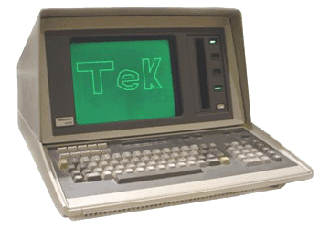
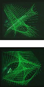
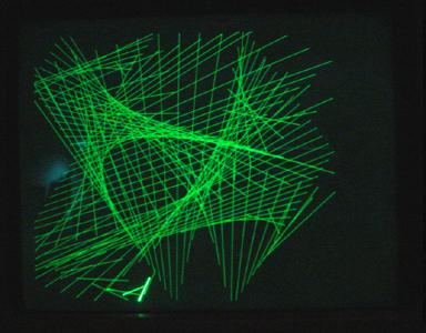
Lines! - This program draws a line and moves it around in a random manner, the DVST stores all the previous positions of the line, which gives an interesting effect. I set up a line counter that would store the number of lines drawn in X, and after 150 lines have been drawn the computer would erase the screen then continue drawing. The picture of the 4052 computer system at the top right of this page was taken using this program. Below are some other pictures of the computer using this program:
In 2025, with the help of ChatGPT, here is a Python script and a compiled executable or screensaver for Windows 10/11 emulating this program!
- Python script
- Windows executable (tested on Win10/11)
- Windows .scr to copy in C:/Windows/System32 (tested on Win10/11)
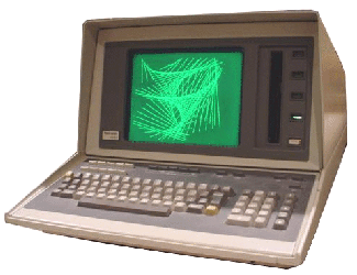
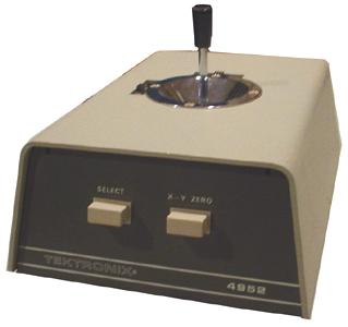
Draw - This program uses the 4952 joystick for the 4052 and a POINTER statement to draw lines. The graphic pointer is moved to a point then one presses any key but Z then that sets the initial point, then the pointer is moved to another location and by pressing any key but Z will draw a line from the initial point to that point. This program can be used to draw images using the pointer. Now about the Z key, when you press Z at a new point, then it will move the initial point to the new position without drawing a line. Basically when you draw lines using other keys, the final point becomes the new initial point for the next line to be drawn. Z simply moves the initial point without drawing a line. I managed to draw a picture of TEK using this program as shown in the following picture.
Spirograph - This program demonstrates the power of the floating point and trigonometric operations on the 4052 drawing a neat spirograph.
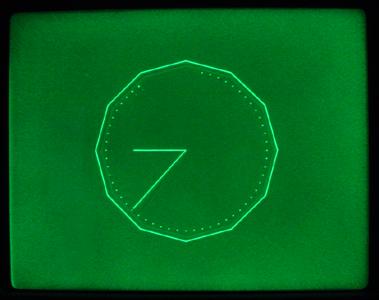
Clock - This program uses the 4052RO9 Real Time Clock ROM Pack that attaches to the ROM expansion backpack on the 4052. The ROM pack extends the BASIC commands to include CALL "SETIME" and CALL "RDTIME" to set and read the time respectively. When the ROM clock has to be set, it requires the information this string format: DD-MON-YY HH:MM (i.e. 01-JAN-06 12:00), so the program simply prompts for the time then injects that into a string with some random date and sets the ROM clock. Afterwards, the program calls a subroutine to draw the face for the clock, then reads the time and stores it in string A$ that follows the DD-MON-YY HH:MM format. A$ is then disassembled to three strings for hours, minutes, and seconds. All of these strings are converted into a mathematical value for arithmetic and logic operations. After the digits have been obtained, the program draws the hour and minute hands. The displayed minute is stored in P, and the seconds are stored in I. Then the minute value is obtained again and is compared with the value in P, and if it is greater (a minute has passed) then the program goes to the subroutine to erase the screen and redraw the clock face, then when it returns it goes to line 130 and from that point on obtains the new hour and minute and redraws the hands and so on. If a minute has not passed, then the program goes to the seconds section to draw the seconds dot for every second (when S becomes greater than the current second stored in I). In short, the clock draws an analog clock and the DVST stores everything so the only processes that takes up most of the computer's time is drawing the seconds and checking for the minutes. When a minute passes, the screen is cleared and redrawn so the hands can be repositioned. Below is a picture of the clock on the screen: the time displayed is 9:37:54. Notice that there is no seconds dot for the 0 and 1 because it takes up a little over a second for the DVST to completely erase when a minute has passed and have the whole clock redrawn.
Monty McGraw has designed a Flash drive that can load many original recovered 4052 programs and demos over GPIB, check out the project page here: 4052 Flash Drive. Videos of the flash drive in action can be found here: Tek Vectors YouTube channel.
When I first built the Flash drive in early 2025, I encountered random issues with programs aborting and seeing a "GP INTERFACE I/O ERROR IN LINE xxx - MESSAGE NUMBER 69" print on the screen. This was resolved with DRAM replacements and a ROM firmware update, refer to Repair Notes and Resources section below. Here's a drawing of the Tektronix logo on my 4052 loaded from the Flash drive.
Repair Notes and Resources
A 1982 copy of the 4052/4054 service manual can be found on archive.org: Tektronix 4052/4054 Service Manual & Technical Data.
When restoring any 4052, it is recommended to obtain or build a 4052-54 diagnostic ROM pack. This module is essential to diagnose firmware start up issues. When I originally repaired my 4052, it was able to start up with a blinking cursor, accept manual entry of very simple BASIC programs and execute them without trouble. I did not try anything else like loading tapes or communicating over GPIB to load or save programs. When I built the GPIB Flash drive, it became more apparent that my 4052 was not fully functional. After obtaining the diagnostics module, RAM tests indicated there were faulty 4116 DRAM that happened to not affect the start up operation and lower sections of memory. Faulty DRAM potentially could affect start up and prevent any display operation on the screen; in this case, the diagnostics pack has LED indicators that can point you in the right direction on where to diagnose failing DRAM.
4116 DRAM failures
The first 32KB of 4116 DRAM are soldered on the board and must be desoldered and removed, and I recommend soldering in sockets for all of them afterwards. There are 4116 DRAM component testers available on Ebay like the following photo that are valuable for testing each chip individually and thoroughly.

My 4052 turned out to have 3 faulty DRAM chips out of the 36 populated chips for a 64KB configuration, or a roughly 8% failure rate. Below are screenshots of the Long RAM tests failing on my 4052, but symptoms may vary depending on exactly where the DRAM failure happens to be and if the diagnostics ROM is using this RAM space.


Once all DRAMs are verified good and installed, the diagnostics pack Long RAM test will pass and looks like this on the screen:

v5.1 ROM firmware update
The diagnostics pack has a ROM CRC test that verifies the integrity of the ROMs on the MAS (Memory Access Sequencer) board. The ROMs I had populated on the board back in 2005 were the first version v2.1 (circa 1978-79) that are known to be buggy. At the time, the ROMs were not electrically or UV erasable so Tektronix designed in a patch ROM and PLA to populate on the board that would decode addresses where there was buggy code in the original ROMs and disable these ROMs while switching over to activate the patch ROM to produce patched data onto the data bus. The patch ROM occupied addresses 4400-47FF. Follow on firmware revisions would be included in a newer set of ROMs and require the PLA + patch ROM to be removed. The final latest and greatest firmware version is v5.1 from 1983 that does not require patches so the PLAs U845, U863) and patch ROMs (U805, U897) are depopulated.
WSI 57C49 EPROMs may be used in place of the original MK36000 ROMs and programmed with v5.1 firmware, the 57C49 address pins are different from the MK36000 but the binaries have the firmware sections transposed to account for the address pin differences. Firmware including raw binary and S19 format can be downloaded here: v5.1_57c49_binaries_tek4052.zip. 57C49 can be programmed on a Data I/O 29B with Unipak 2.
| U# | Tektronix Part No | Jos' MAS_4052_57c49 EPROM HEX Motorola S-Record filename |
MAS board address range |
|---|---|---|---|
| U810 | 160-0260-03 | 57c49-0260-03.S19 | E000-FFFF in RAM space - EVEN ROM |
| U820 | 160-0261-03 | 57c49-0261-03.S19 | 4000-7FFF in ROM space - EVEN ROM |
| U825 | 160-0262-03 | 57c49-0262-03.S19 | 8000-BFFF in ROM space - EVEN ROM |
| U835 | 160-0263-04 | 57c49-0263-04.S19 | C000-FFFF in ROM space - EVEN ROM |
| U870 | 160-0264-03 | 57c49-0264-03.S19 | 4000-7FFF in ROM space - ODD ROM |
| U880 | 160-0265-03 | 57c49-0265-03.S19 | 8000-BFFF in ROM space - ODD ROM |
| U885 | 160-0266-04 | 57c49-0266-04.S19 | C000-FFFF in ROM space - ODD ROM |
| U893 | 160-0267-03 | 57c49-0267-03.S19 | E000-FFFF in RAM space - ODD ROM |
Note that the earlier MAS boards need further modification to ensure v5.1 ROMs operate correctly. v5.1 firmware has code in the patch ROM space 4400-47FF that require the patch ROM space to be disabled and this is shown in the final revision of the MAS schematic. The modification requires disconnecting U280 pin 5 and 6 from the board and grounding pin 3 of the ROM address decoder U420 and U470.
Symptoms of upgrading to v5.1 firmware without any board modifications include fatal "SYSTEM ERROR" messages like these screenshots:


Also the modification to disconnect U280 pin 5 and 6 is critical because otherwise U280 will try driving into a short circuit to ground. This may not result in any observable symptoms when using the computer normally, but I observed a fatal crash when running the diagnostics pack ROM CRC test as soon as it hit the U805 patch ROM space causing U280 to drive into a short circuit and probably caused the 5V rail to sag and affect other chips. Below is a screenshot and short video of the failure symptom:

After successfully upgrading ROMs to v5.1 and applying the necessary modifications on the MAS board, the expected ROM CRCs that match what others have seen on their 4052s are shown in the following screenshot:

More detailed writeup on the firmware upgrade process is documented in this post on VCF: How to upgrade tektronix 4052 or 4054 with latest v5.1 firmware.
An observation about early MAS boards
The MAS board in my 4052 is dated 5/10/79 and there is usually a small white sticker after the part number 670-6030- printed on the board to indicate its revision, found near the lower left corner of the board. Mine appears to be missing a sticker and may be either a prototype, first revision 0 that never had a sticker or the sticker fell off. Considering that I obtained it from a former Tektronix employee, it is very possible that he had access to purchasing prototypes or early revision models.

More importantly, my early revision board does not have U265 (74S10) footprint, but the chip actually exists and was piggybacked on top of U450 (74S00) as shown in the following photo. I do not know if this modification was done by the factory, but it appears professionally done and matches the later 1983 revision of the MAS schematic.

Later revisions of the MAS board have a U265 (74S10) footprint placed next to U260 as seen in this example photo of a -09 revision, and there's no longer a chip piggybacked on top of U450 with wiring.

The following schematic diagram shows the ROM control circuit of an early 4052 taken from a 1978-79 Tektronix 4052 Service Manual that matches my board, and the pair of pencil-drawn 3-input NAND gates is a 74S10 that represents U265 on later revisions and is the piggybacked chip on top of U450 with rework wiring seen on my early MAS board. U450A and U450B were the original decoders for ROMs U810 and U893 respectively, but did not take in account the FPLA patch FLAG signal as an input - this was either an oversight or the designers didn't anticipate needing to apply a patch to these ROMs. The outputs of U450 pin 3 and pin 11 were disconnected and driven by the new 74S10 outputs.

This drawing also shows the modification to disconnect U280 pin 5 and 6 from the board and grounding pin 3 of the U420 and U470 decoders that are required for the v5.1 firmware update. For reference, later revisions of this MAS schematic for the ROM section look like below with U450A/B removed from the drawing and U265 added (highlighted in yellow), but the aforementioned modification for U420/U470 are necessary:

Other hardware ailments
My 4052 at one point in time experienced a PCB vias failure on the display board for the -20V rail resulting in no visible cursor on the display, but I knew it was not a computer problem because it was working before the vias failure occurred. The high level failure symptom I saw on the display was a dot in the center of the screen on power up. I noticed if you hit any character key repeatedly then suddenly the characters would start appearing but only as flat lines past the center point, and if you hit the Return key repeatedly to position the cursor to the lower right quadrant then the characters and cursor would appear on the screen normally. It looks like this:

Digging into the display board, I measured the I/O board producing X and Y deflection voltages in the range of approx +/-8V. The lower right quadrant of the display correspond to X and Y voltages that are below 0V (e.g. top half is Y>0V, left half is X>0). I traced the XY voltages from the I/O board through the amplifiers and noticed the final output stage that is powered by the unregulated +/-20V died when deflecting below 0V indicating a -20V rail failure. Also there is a 5.1V zener regulator off -20V to provide a ~-15V bias that was measuring +10V with respect to ground. What was puzzling to me at first was I had measured -20V as expected at the connector pin 8 of J54 on the display board. All the other power supply voltages at this connector even checked out OK. It wasn't until I measured the zener voltage that I realized -20V was not making it to the rest of the board and found a disconnection at the vias where the trace transitioned to the other side of the board. The fix was simply soldering in a jumper wire from the vias to a -20V point in the deflection circuitry, like this:

Other possible failures unrelated to what was noted above have been documented in this post: Tektronix 4052 troubleshooting.
Back to Top