Relay Computer Two
"There was a space program before there were integrated circuits." - Jack Kilby
Return to Home
Return to Projects
Interested in building relay logic circuits? Consider buying Catahoula Technologies Relay Logic Modules and read more about them in the Relay Logic Projects.
Why on earth build a relay computer when there are already computers over a hundred thousand times faster? Well, for two reasons: to prove that silicon is not magic and because I wanted to.
The simple relay adder was built using free NOS relays sometime in 2005, but my goal was to someday build a more elaborate one that could run programs but not fill up a room like the early computers. Harry Porter built an incredible 415-relay computer which can be seen at this page: http://web.cecs.pdx.edu/~harry/Relay/
I never thought I'd fully understand how his computer worked, let alone build one. Finally in spring 2007, I gained more understanding of computer systems from a course in college then joked to a friend about using the x86 instruction set for a relay computer to boot up Windows, which would’ve taken several hundred years on a relay computer running on a 50Hz clock. And so the inspiration began... (note: if you want to skip the hardware details of the computer, the pictures and videos are at the end of this page).
Seriously, the x86 instruction set is insanely large for a simple relay computer so I created my own instruction set. I looked at Harry Porter’s relay computer design for inspiration and ideas for the hardware. But first, the computer cannot exist without the actual relays. After searching several online electronics suppliers for relays, the lowest price I could find was at $1 per relay so a computer using 200+ relays can become rather expensive. So ebay was the next option and after patiently watching several auctions, a lot of 168 SPDT relays came up and I nabbed it for about $25. A few weeks later, another lot of 100 4PDT relays came up and I won it for about $14. Including shipping costs, the total cost for the 268 relays I purchased from ebay was about $60. So, 268 relays became my limit for the computer design. Obviously, I did not try to copy Harry Porter’s relay computer because it called for 400+ relays, but I borrowed many ideas from his design so I wouldn’t have to reinvent the wheel. During the weekends at school, the relay computer was designed with a limit of 268 relays (which eventually increased to 281 relays), a 8-bit data bus, a 16-bit address width, and a floating zero. Moreover, I created my own instruction set architecture (ISA) using only 5-bit instructions for simplicity.
One might wonder "what the heck is a floating zero?" There is a significant difference between using a grounded zero compared to a floating zero in relay logic. The grounded zero means the zero is represented by a connection to the power supply ground. This can simplify certain logics such as the XOR, which would need only one relay. My first relay adder used the grounded zero. However, the grounded zero poses problems with other logics such as the memory registers due to the potential of shorting out the power supply. I circumvented this problem in my first relay adder by using resistors. A floating zero basically means there is no connection to the power supply ground, positive source, or anything, hence the name "floating" zero. This is hugely beneficial for avoiding shorts when the relays change states, especially in the registers.
Before continuing to the details of the relay CPU hardware, the hardware is based on the instruction set architecture (ISA) chosen. My ISA is basically classified in four different categories: Branch, Data Movement, ALU Function, and Halt and the exact instructions and definitions may be viewed here: Relay Computer Two ISA.
The relay CPU architecture is shown below:
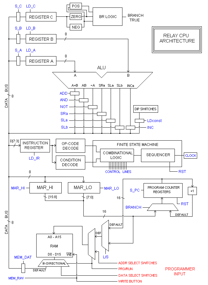
The three registers and the ALU
The first step was to build the three CPU registers: A, B, and C. Below is a schematic of a single 8-bit relay register:
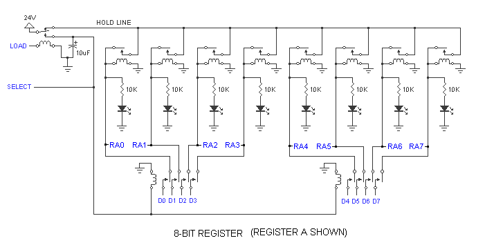
The register works based on electrical latching. When the HOLD line is high then if the memory relay coil is activated, the switch closes and keeps the coil activated. When the HOLD line is turned off, that is, disconnected from the positive supply source, then the coil is unable to remain energized and the switch opens. So to load from the data bus, the LOAD input is set high and the relay disconnects the HOLD line from the positive source, thereby allowing the memory relays to clear, and connects the SELECT line to the positive source to connect the data bus to the register. The memory relays change states to correspond to the data on the bus, but they do not latch the bits until the HOLD line goes high. In theory, when the LOAD line goes low, the HOLD line goes back up and the bits are stored. However, this is not always so because there is a tiny time gap for the relay to switch from SELECT to HOLD during a load, so the data bus could be disconnected before the memory relays are able to hold the bits. To prevent this, a 10uF capacitor is placed on the SELECT line to keep it active milliseconds longer so the HOLD line has a chance to go back high so the memory relays store the bits before the data bus is disconnected. This register design is also used for the Memory Address Registers (MAR_HI and MAR_LO), and the Instruction Register (IR) except only 5 bits are used rather than 8.
After constructing the three registers, the ALU was the next step because the functions derive their inputs directly from one or two of the registers. The ALU functions include: A+B, A AND B, NOT A, SHIFT RIGHT A, SHIFT LEFT A, SHIFT LEFT B, INCREMENT A, and LOAD CONSTANT (ADDab, ANDab, NOTa, SRa, SLa, SLb, INCa, LDconst respectively are the mnemonics of the ALU functions in the ISA). The third register, the C register, is the destination register for all ALU functions to keep the control circuitry simple. Another reason for setting C as the destination register is to avoid possible errors. One big difference between the relay registers and modern solid-state registers is that they do not basically shift in data as the old data shifts out. Once data is written to a relay register, the old data is lost before the load actually occurs. This poses a serious problem when writing the result of an arithmetic function back to one of the source registers. For instance, the NOTa function produces a result based on the contents of register A. If the result is written back to register A, then the contents in A are lost which causes the result of NOTa to change, which can cause undesired oscillations. To circumvent this, all ALU functions are sent to register C because it is not a source register.
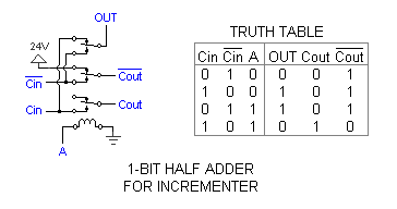
The 8-bit adder is based on Konrad Zuse’s design and is quite ingenious. A single bit adder consists of two 4PDT (four pole double throw) relays with two carry inputs (one is the inverse of the other). To do a simple add, Cin and Cin’ are 0 and 1 respectively. To increment register A, the data from register B are disconnected from the input of the adder so it only sees register A. Then Cin and Cin’ are reversed to 1 and 0 respectively, and the output is the increment of A. Below is the circuit for a 1-bit adder.
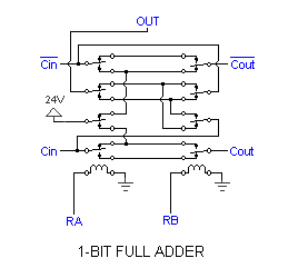
Each 1-bit adder is cascaded as shown below to form a 8-bit adder and incrementer.
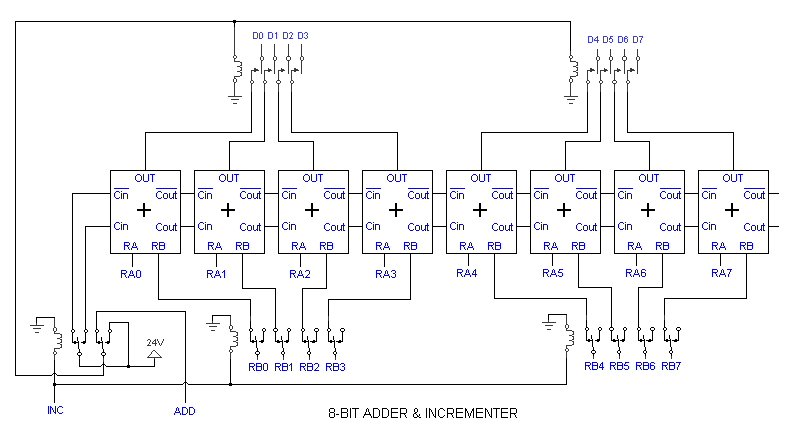
When INC is activated, the DPDT relay (or two SPDT relays) at the bottom left will activate the relays that disconnect register B from the input of the adder so it basically adds register A with zero. Moreover, the relays at the bottom left will feed a logic 1 into Cin (Carry Input) of the adder, which automatically turns it into an incrementer. At this point, the output of the adder is register A plus one. On the other hand, when ADD is activated, that simply connects the output of the sum of register A and B onto the data bus.
For the 8-bit logic unit of the ALU, ANDab and NOTa use 16 SPDT (single pole double throw) relays in the following circuit configuration. Note that only the first four bits are shown.
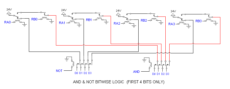
Observe that AND only outputs a logic 1 if both inputs are 1, so for instance, the pair of relays for RA0 and RB0 must be activated for a logic 1 to switch through to the output. NOTa is done simply by using the normally closed (NC) contacts of the RA relays so when RA0 is zero, a logic 1 will be present on the NC contact.
The shift logics are quite simple. Below are the schematics for the SRa, SLa, and SLb logics.
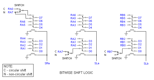
Notice that there are switches, not relays, in the circuit that select circular or non-circular shifts. For a left shift, circular means the input MSB (most significant bit) is moved to the result LSB (least significant bit) while all the other bits shift to the left. Switching to non-circular simply disconnects this "loop" and the input MSB is simply dropped off and the result LSB is loaded with zero (remember, the zero floats). For the right shift, the LSB of the input is moved to the MSB in the result for circular mode. In non-circular mode, the switch simply disconnects the input LSB from the MSB of the result, and connects the result MSB to bit 7 on the input to sign-extend. The MSB of the input represents the sign of the number, whether it is positive or negative, so if we shift right, we need to keep this sign in the front so we simply copy this in place of the result MSB. The switches allow for a little bit of hardware programmability, because circular or non-circular shifts have their benefits in certain applications.
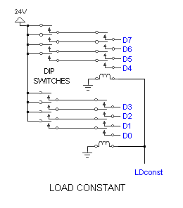
The final ALU instruction is LDconst, which basically loads a constant in register C. This instruction is used to load a commonly used constant for a program because the instruction takes half the machine cycles needed by an instruction used to load from memory. DIP switches are used to select the constant, but for most of the time it is set at -1 or xFF (2’s complement for -1). Below is the schematic of this circuit.
The Program Counter and Memory Address Registers
One might wonder, why a 16-bit address bus for a relay computer running on a clock rate that is over several thousand times slower than most computers in the seventies? 16-bits means 64KB of memory, and most personal computers in the seventies didn’t even have 8KB of memory! It would make more sense to limit the address width to 8 bits to match the data bus width, but that is only 256 bytes of memory. It might seem like plenty for one program, but I had planned on using a NV-SRAM (non-volatile static RAM) so I could store programs and not have to enter them in memory ever again so 256 bytes can be quite limiting. Expanding the address width to 10 or 11 bits would make better sense, but with absolute addressing it is a bit of a mismatch with a 8-bit data containing the first 8-bits of the absolute address and the next 8-bits of data with the first few bits for the upper n-bits of the absolute address. So I figured I’d go the whole nine yards and use twice the data bus width for the address width, so 16-bits for the width.
The Program Counter, or PC for short, is a 16-bit register that stores the address of the CPU location in memory. This location is used to retrieve instructions or data from memory for execution. As the CPU executes the current instruction, the PC generally increments to the next location so the CPU can fetch the next instruction when it is done executing the current instruction. A 16-bit incrementer is used to increment the PC, using only 16 relays plus a few supporting relays. The following schematic is a half adder (a revised form of the full adder used in the ALU where the second relay is left out). An increment is achieved by feeding 1 and 0 in Cin and Cin’ respectively at the first half-adder. The output will be the incremented input.
By connecting the PC directly to the inputs of the incrementer, one can load the output of the incrementer into the PC to increment the register. However, it is not as easy as it seems with relays. The relay register as discussed in the ALU section do not act like solid-state registers and cannot simply load a new value if its current contents are being used to create this value. Simply put, loading the output of the incrementer to the PC register while its current contents feed into the incrementer will result in a closed loop then the incrementer will go off wildly incrementing itself and make the relays buzz. This problem can be compared to using a solid-state latch with the output connected to the input. There are several solutions to this issue.
Harry Porter used a second PC register for a master-slave flip-flop configuration to break the loop between the PC and the incrementer. This will be explained shortly. I hated the idea of using a second PC register because it uses 21 relays (16 SPDT for bit storage, four 4PDT for enable, and one SPDT for enable/hold control). The idea to eliminate the second PC register was to use capacitors to hold the bits of the current PC to feed the input of the incrementer. Then the PC is quickly disconnected from the input of the incrementer and loads the output of the incrementer before the capacitors lose their charge. This is very much like how dynamic RAM works. Below is a schematic of a 4-bit PC incrementer that worked based on this idea.
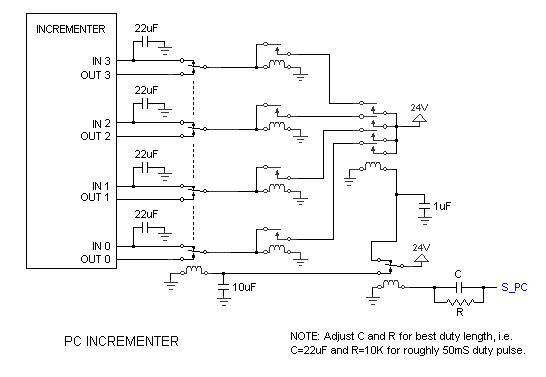
Once the PC incrementer went beyond 5 or 6 bits, it began to malfunction because of relay hysteresis. Relay hysteresis (meaning lag) is when relays do not switch off immediately after power is removed due to magnetization in the coil and other inductive kickback effects. Notice that the HOLD line has been replaced with a 4PDT to individually switch power to each bit storage relay to help overcome hysteresis effects. I noticed that during the quick load cycle, some relays tend to turn off slower than others turn on. Suppose the PC was going to load 0100 and the existing PC is 0011, if the lower two bits do not turn off as quickly as the third bit turns on, then the HOLD line could be pulled up and keep the other bits on, resulting in a transition from 0011 to 0111. The 4PDT that replaces the HOLD line prevents this. Overall, for a circuit like above that is all based on delicate timing, hysteresis becomes an annoying problem that can only be overcome by using a longer duty cycle. Unfortunately, a longer duty cycle means the capacitors have to be larger in order to hold the bits long enough before it is lost. Thereby, the whole circuit becomes too slow and unreliable. However, this is a pretty nifty circuit for a simple 4-bit binary counter.
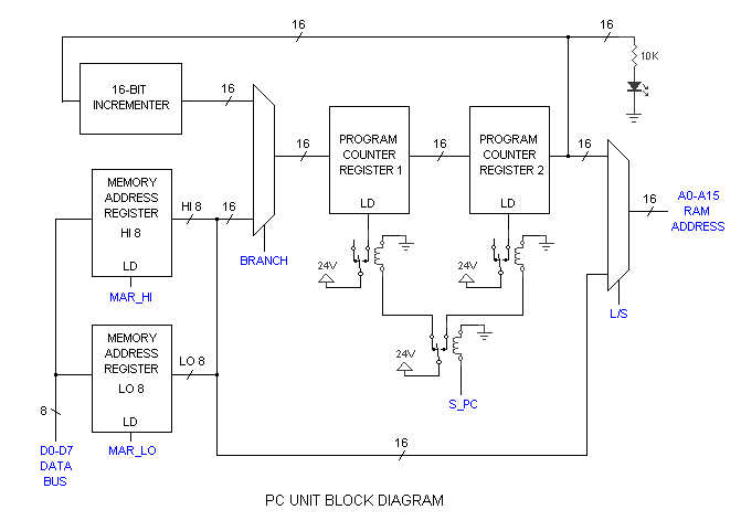
A second PC register (PCR) was used, despite the extra 21 relays, because it was more reliable. PCR2 constantly feeds into the incrementer. To increment PCR2, PCR1 loads the incremented PCR2, then PCR2 can safely load PCR1 to increment without closing the loop. To achieve this, there must be a dead gap between loading PCR1 and loading PCR2 to allow the relays to settle. Moreover, I did not want to design the finite state machine to control the loads of two PCRs so I used three SPDT relays to combine the two load signals in a single input signal. While relay hysteresis was undesired in the previous PC increment idea, the use of relays to control the two load signals take advantage of hysteresis to provide a safe gap between the loading of PCR1 and PCR2. Below is a block diagram of the PC unit in my relay computer that has all the associated components for addressing.
The schematic for the PC unit is shown below, and each half-adder block uses the circuit shown several paragraphs back. Note the schematic does not show every single component in the PC unit, but the dots imply repetition of the same circuit and wiring for each respective address and data bit.
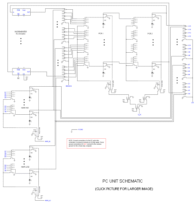
Note that when power is applied, the relays will put PCR2 in a load state, while PCR1 is in a store state. When a signal is applied to S_PC, the relay will switch power to activate the load relay for PCR1. However, due to relay hysteresis, the instant S_PC goes high, PCR2 will start the load-to-store transition quickly while the other relays eventually activate PCR1 in a load state. Finally when S_PC goes low, the same thing happens in reverse, and data from PCR2 has moved to PCR1 successfully. I observed that if PCR1 is in a load state and PCR2 in a store state, this becomes problematic because PCR1 will set its bits to the output of the incrementer and if a BRANCH instruction is true, the mux will switch the input of PCR1 so fast that it is unable to clear itself before changing its bits to the contents of the MARs. This often resulted in the address of PCR1 and the MARs becoming OR’ed together. The fact that PCR1 goes in a store-to-load transition actually gives it time to clear before loading the new bits. Relay hysteresis can be a pain in the neck or advantageous.
With no signal on BRANCH, PCR1 will load the output of the incrementer, which increments the contents of PCR2. If we wish to branch, then BRANCH goes high, and PCR1 will load the output of the two memory address registers (MAR). The reason for using memory address registers is because absolute addressing will require a specific 16-bit address, but the data bus is only 8-bits wide. Thereby, we load the upper 8-bits of the 16-bit address from the data bus (from memory) into MAR HI-8, then the lower 8-bits of the address from the data bus into MAR LO-8. For a branch instruction, BRANCH will go high, then we activate S_PC to load PCR2 with the 16-bit address from the two MARs. For a LOAD or STORE instruction, we do not want to alter the contents of the PCR so we simply activate L/S and retrieve or store data at the address stored in the MARs. After that, L/S is deactivated and the memory goes back to the address stored in PCR2 for the next instruction.
Finally, note that all the ground connections for the PC unit as shown in the schematic above are local and all connect to the PCGND signal. These ground connections do NOT connect to the common ground of the whole relay computer. The finite state machine has a relay that connects or disconnects PCGND from the power supply ground to clear the PCRs and MARs for a HALT instruction or a manual reset. This way the computer can start back at address x0000 in memory when resetting the CPU after a HALT instruction.
The Finite State Machine
The Finite State Machine (FSM) controls all the aspects of the relay CPU like a conductor runs the orchestra. There are two parts to the FSM in all computers, the combinational logic and storage. In this relay computer, there is a sequencer (the storage component) that is basically a 12-state linear counter. The sequencer increments the state for every change in the clock; in other words, both a rising and falling edge of the clock triggers the sequencer. The relay logics decode the current state produced by the sequencer plus the instruction stored in the 5-bit instruction register to control all the subcomponents of the relay CPU, including the ALU and the PC unit.
Below is the schematic of the 12-state sequencer used in my relay computer:
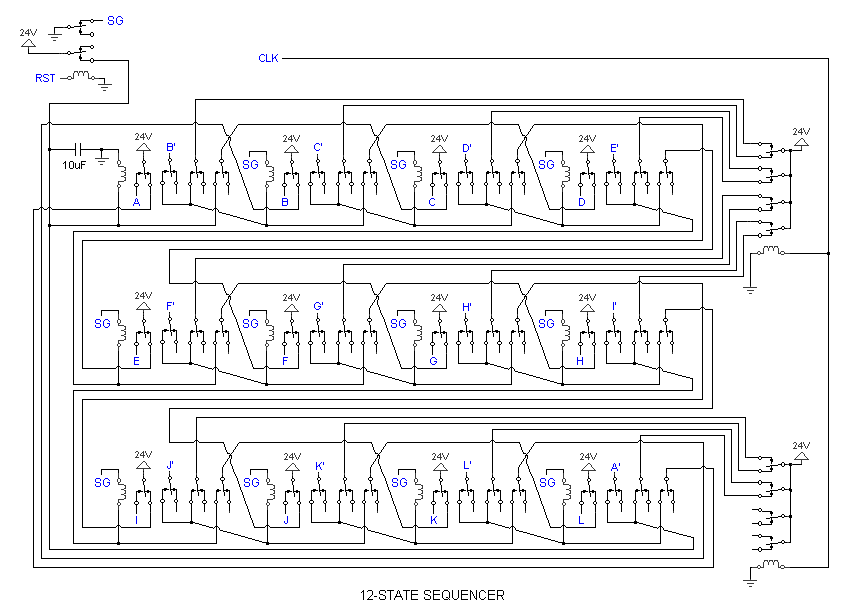
The circuit was devised by Harry Porter and is quite neat, but I simplified the reset circuitry. The sequencer produces different timing pulses that can be used by the combinational logic as shown in the timing diagram below:
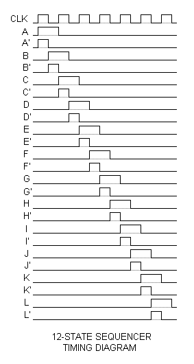
The LEDs are connected to all the primed letters (signal connections, i.e. A’) to reflect which state the sequencer is in. When RST goes high then low while the CLK signal is low, the LED for A' should light up. If CLK is high while RST goes high then low, the sequencer will freeze so it can only be reset at certain times.
The instruction register (IR) is a 5-bit register with the upper two bits as the op-code and the next three bits as the conditions. The IR loads the instruction off the data bus from the RAM in the first state and anything in the lower three bits of the data bus are ignored. It is built exactly like the 8-bit register used in the ALU, except the first three bits (D0, D1, and D2) are left out. The inputs of the binary decoder are wired to the IR, i.e. RA3 to RA7 in the 8-bit ALU schematic. In the following schematic, these connections are labeled as IR3 to IR7, instead of RA3 to RA7 for your information.
The combinational logic was designed to be really simple so the same relays could be reused for different instructions, such as the condition decode relays. However, this part of the CPU is very tricky and difficult to simplify due to the nature of relay switches being bi-directional. For solid-state components such as a transistor, a signal on the input can activate the output, but not vice-versa. This is not true for relays; the switch can conduct current in either direction so if the logics are not designed with care then current could travel through various switches and connections causing the CPU to behave unexpectedly. Harry Porter calls this problem "backdriving." Nevertheless, after hours and hours of experimentation and testing, I eventually debugged most of the logics in the FSM to prevent surprising behavior, and below is the schematic (in three parts) of the relay logic I came to use:
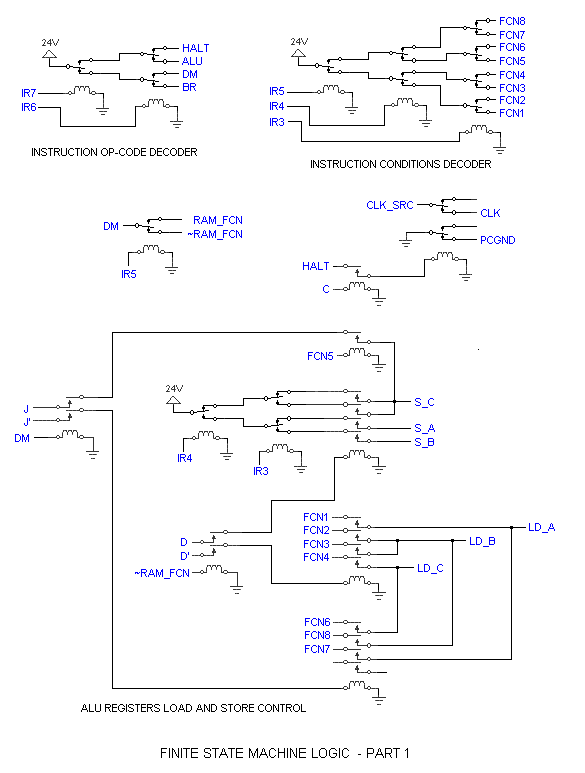
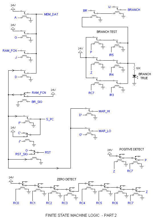
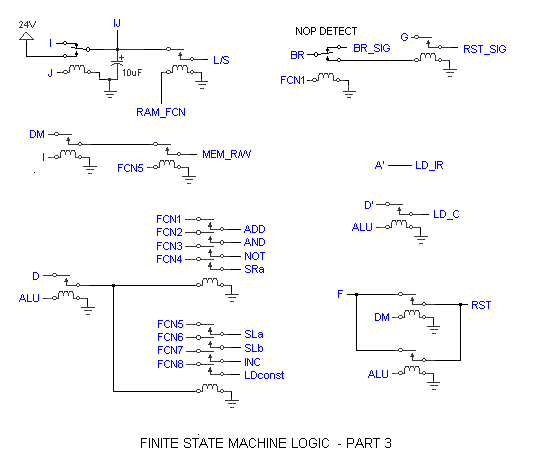
Note that LD means LOAD, i.e. LD_A connects to LOAD of register A, and S means Select, i.e. S_C connects to SELECT of register C. It is quite difficult to explain how the logics work, but to make sense of how or why it works, the instruction timing diagrams below can be very helpful:
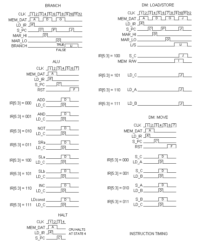
The RAM
The RAM I used is solid-state, so yes I admit this is not a 100% pure solid-state-free computer but the CPU is all relays. There are many reasons for using solid-state RAM. The obvious reason is because building RAM out of relays, core memory, or something is really difficult. Imagine 256 bytes of relay RAM, which is 2048 bits and not to mention the address decoder and everything else. Even if it was possible to use one relay per bit, 2048 bits for a mere 256 bytes of RAM is just simply expensive. Core memory was another consideration, but many geeks consider them collectibles and pay big bucks to obtain a small 16x16 matrix to put in a pretty little frame. Then there is the thought of buying a jar full of the ferrite doughnuts for a few bucks and make my own.
So, I initially planned to use a Dallas DY1220 2KB non-volatile SRAM so I could store my programs in memory without ever having to reprogram the memory every time the computer was shut off. I planned on using a 32KB SRAM, but 2KB seemed satisfying and the CPU was designed for 64KB so at least it has expandability. I had another idea for simplifying the CPU by expanding the IR to 8-bits and use the last three bits as part of the address, but I had already built most of the CPU before I even thought about it, but the ideas will be explained later below.
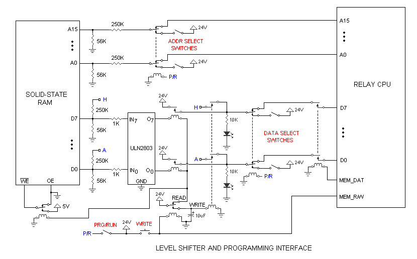
The challenge was to devise a level shifter to interface the RAM to the relay CPU. The RAM runs on 5 volts, so a logic 1 is 5V and logic 0 is 0V. The relay CPU uses 24V for a logic 1 and a floating connection for logic 0. The level shifter takes care of the differences like a money exchange for two currencies.
I attempted to save parts so the level shifter was a bit tricky to design. The CPU-to-RAM converter was basically in parallel to the RAM-to-CPU converter. One or the other was simply active during a read or write, but there is the potential of closing a loop between the two converters, resulting in latched bits. After design number 5 or so, I eventually bought several 5-volt reed relays for the converter. However, the use of reed relays was a huge mistake because those relays are very sensitive to magnetic fields around them. In fact, I hooked up an ohmmeter to the reed relay contacts and energized the coil. There was continuity, but when I brought a small weak magnet about a half inch away from the relay, the switch opened! After a couple weeks of struggle to shield the reed relays with sheet metal and ensuring they switched properly, I gave up and bought REAL 24V relays from a local electronics store. The final design worked with these relays, as shown below:
The RAM block actually can be composed of several smaller RAM chips, or memory mapped input/output (I/O) devices. I used a 74HC138 and 74HC133 to memory map eight possible I/O devices. Below is the schematic of the RAM block:
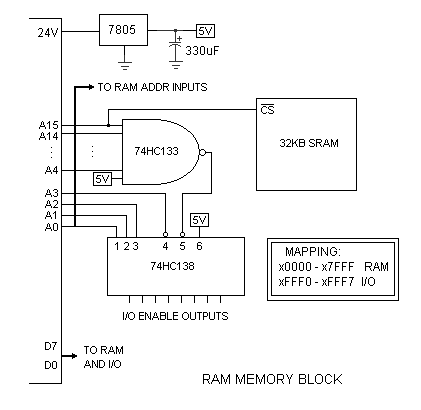
The Power Supply
Of course nothing works without a power supply. Below is the schematic of a regulated 24VDC power supply using minimal parts and is capable of supplying up to 2.5A, which is roughly the peak current consumed by the relay computer depending on the clock speed and the contents of all the registers at a time. 24V at 2.5A maximum is roughly 60 watts peak, and on average, the relay CPU consumes about 40 watts.
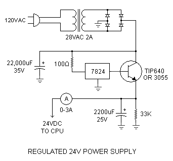
That is all there is to it! The relay count and costs are below:
|
RELAY COUNT
|
COSTS
|
Lessons Learned
Below are a few tips so you don't repeat my mistakes if you decide to be crazy enough to build a relay computer.
- Don't bother with a 16-bit address. In retrospect, I decided this was way more memory than necessary for a slow computer. Had I built this CPU a second time, I would opt for 8-bit addressing and keep the memory at 256 bytes. 9 to 11 bits is also reasonable and recall there are 3 unused bits in the instruction bytes that can be reused. There are several advantages with reducing the address length. First, less sequencer states would be necessary because there is less to transfer from memory to the Memory Address Registers. The PC and its incrementer would be reduced in size and save a lot of relays.
- Examine the instruction timing diagrams carefully and try not to cut corners when loading data into registers. The computer was not exactly 100% reliable over time due to relays starting to stick after operating for a while and causes unpredictable erroneous behavior.
- Some instructions are not as useful as I initially anticipated so there is room for improvement there.
- Make sure the clock that operates the sequencer is around 50% duty cycle. Any imbalance can cause switching issues because the sequencer advances on both "rising" and "falling" edges of the clock. I did not include a schematic diagram of the clock here because it can be built in any number of ways you prefer. I originally used a function generator that controlled 24V to generate the CLK signal, and then made a single relay oscillator that ran very slowly as the final solution.
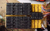
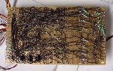
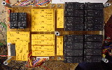
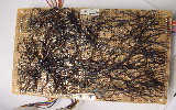
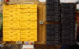
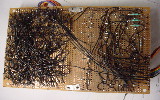
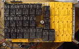
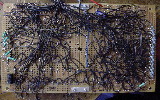
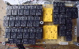
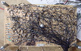
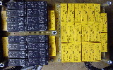
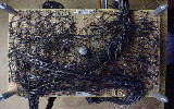
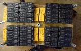
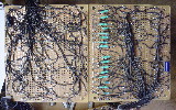
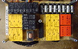
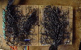
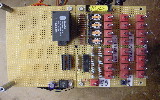
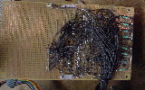
Pictures of the relay CPU are shown below. The first series of thumbnails (click for larger picture) show each section of the computer plus the bottom view wiring. The completed computer photos can be found near the end of this page. Enjoy!
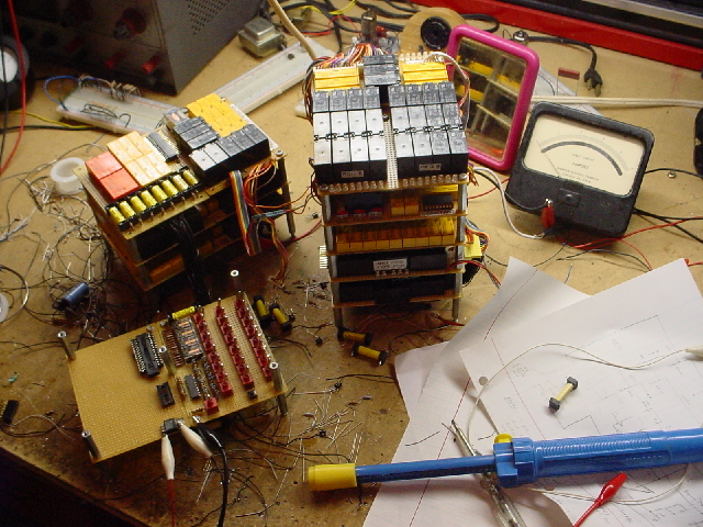
The whole computer as of 6/8/07
The video shows the CPU running the program shown below:

The program assumes that register A is already clear, which is the case during power-up.
The video shows the CPU running the program shown below:
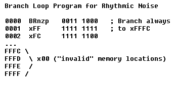
The 32KB RAM is only active from x0000 to x7FFF, so when the CPU branches to xFFFC, nothing is returned on the data bus. This "nothing" or x00 is interpreted as a NOP (no operation) by the CPU, so it simply increments the program counter until an instruction appears. However, as xFFFC increments to xFFFD, xFFFE, xFFFF, the 16-bit incrementer overflows and the PC goes back to x0000. Voila, the CPU is back to the branch instruction that sent it to xFFFC. Sounds like the most worthless program, a branch that loops back to itself. However, the fact the PC changes from the low end of memory to the high end of memory causes the clicks to get heavier. Also, when the PC loads a lot of bits, i.e. xFFFC then the current draw increases dramatically. Also, the computer's clock is gradually increased from around 6 machine cycles per second at the beginning of the video to around 30 machine cycles per second near the end of the video. Beyond 30 machine cycles per second, the relay CPU will start losing bits and go haywire.
I apologize for the slight mismatch in the clicking sound and the clips because they were recorded separately.
This video shows my early and failed attempt at sending characters to the VFD (vacuum fluorescent display) with the relay CPU. The VFD was supposed to be the original output device rather than the LEDs on the relay computer. The problems were due to switch bounce, which causes characters to be sent multiple times and garbage also appears randomly on the display. After the first attempt to display "HELLO!" you can see a screwdriver readjusting the debounce circuit. I also tried speeding up the clock to supress some debounces, which also failed. Never got around to fixing this problem.
Back to Top
