Nixie Clock Version 3
Return to Home
Return to Projects
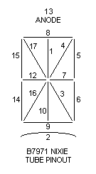
I originally planned on using a Mostek MK50250 6-digit clock chip that multiplexes the digits. However, after trying the chip out with two nixies, I found that the brightness was not very strong. The duty cycle of the chip's output is less than 15% if I remember the datasheets correctly. I tossed this idea out and decided to drive the nixies directly, using 4511 BCD-to-7segment decoder chips. If I had any 74141s or 7441s, I would have used them in place of the 4511 and the MPSA42 high voltage transistors. One advantage to use what is essentially a binary clock with 7-segment decoders is to have small neon bulbs (or LEDs) driven directly from the BCD outputs. I planned on placing the neon bulbs under each digit, so if you're plain then look at the B7971s and if you're a geek then look at the binary below. However, that didn't work out due to complications with the circuitury and the amount of room in the clock case I made.
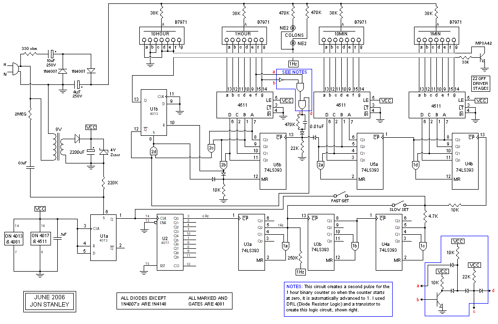
Click here for the schematic diagram of the four B7971 nixie clock.
I experimented with using 74LS393 dual binary counter chips. In the process of constructing the clock, I found that these chips were extremely sensitive to noise. If you used 60Hz from mains and fed it into the 4013, there was still some noise passing through that would make the 74LS393's go haywire. I never had a problem with this in my other two clocks that run off mains, and I discovered the reason after taking a closer look at the datasheets. The 4017 datasheet says the chip was designed to have a strong tolerance for noise, and there is no mention of this in the 74LS393 datasheet. I figure since the latter was normally used in older computer systems, the power supply and input signals are expected to be well-filtered and free of noise. I originally used a 74LS393 to divide 60Hz to 4Hz (without using an AND gate so the chip recycles at every 15th count), and a 4017 to divide 4Hz down to 1Hz. After discovering this noise problem, I swapped them around. I used the 4017 for the first stage to divide 60Hz to 10Hz. I figured that with the 4017 in the front, it would buffer out more of the noise and generate a cleaner clock pulse for the 74LS393 chips. This configuration helped solve the problem.
I designed the clock circuitury hoping to achieve a perfect design that uses all of the logic available in all of the chips I would need. In other words, I did not want to waste one or two AND gates or a whole half of a 74LS393 in the design. I came to a point where I thought I had gotten the design, so I proceed to build the clock. After overcoming the noise problem with the 74LS393s in the clock, I learned of another minor design issue. The 74LS393 clock input triggers on a falling-edge of a square wave (when the square wave signal drops from a logic 1 to 0). The 4017 and 4013 triggers on the rising-edge. It took some experimentation before I could get the signals to work correctly between the chips.
For the ten hours, I didn't want to waste another 74LS393 and 4511 chip just to display zero and one. Zero and one in 7-segment form shares segments B and C, so I hardwired B and C to ground. The other segments for the zero are all wired together and switched on and off by a 4013 flip-flop. As a result, when the clock is turned on, the 1 is always on. The "C" that is switched on to make a zero comes on when the clock is in the single digit hours. When the clock goes to 10, 11, or 12, the "C" is turned off so the digit 1 appears.
I realized a design flaw when I finished the clock. The fundamentals of my binary clock circuitry was based on Hans Summer's binary clock, but his operates in 24-hour mode. I personally prefer 12-hour mode. I was faced with the problem of the clock starting at 00 hours, but the clock does count nicely to 12 and resets back to 00:00 a minute after 12:59. So much for the "perfect" design that used all of the chips wisely. I figured that if the clock was going to roll over to 00 hours, I'd need a "double" pulse to get the hours to automatically advance to 01 hours. As you can see in the schematic, the portion marked in blue uses two AND gates and one inverter gate. Most chips come with four AND gates in one, or 6 inverters in one. This would've been a bad waste of chips, so I decided to do the remaining logics the old school way... DRL (Diode Resistor Logic).
I found a "trait" of the 7-segment zero digit, segment F has to be on and segment G has to be off. None of the other digits have this trait. The inverter using a transistor and resistor changes the "off" G into a logic 1 for the AND gate. The two diode AND gate, one connected to segment F and one to the inverted segment G, will produce a logic 1 only when segment F is on and segment G is off. The reason is because if segment F is off or segment G is on (inverter produces a logic 0), then the diode(s) will pull down the output to ground and produce a logic 0. Therefore, both diodes have to have a logic 1 in order to allow the output to rise to a logic 1. The same DRL circuit is used again to "AND" the 1 hour zero and the 10 hour zero. So, when the hours runs to 13, the AND gate will reset the hours to zero, then the DRL will produce a logic 1 because it senses 00 hours. Although DRL is rather crude and simple, it is very effective and FAST. Without the 470K resistor and 0.01uF capacitor, the pulse from the 10 minutes counter would just drown out the pulse from the DRL. Recall that the 74LS393s trigger on a falling edge, not a rising edge. I think if the 74LS393 operated on a rising edge, the circuit might work without the capacitor and resistor. However, I had to delay the pulse from the DRL until the 10 minutes counter finished sending its clock pulse to the 1 hours counter. The pulse goes high then low, and the falling edge triggers the 74LS393. Then the DRL output goes high so the capacitor starts to charge up. This current draw will pull up the clock input of the 74LS393 to a logic 1 momentarily. When the capacitor stops charging up, the 22K pull-down resistor pulls the clock input down to a logic 0. This falling edge triggers the 74LS393 to advance one more time. There, you have it, a "double" pulse to get rid of the 00 hours.
I built a case out of cedar, and the amount of space I had inside the case was rather limited so I was unable to pursue my idea of using neon bulbs or LEDs for displaying the binary time directly from the 74LS393 counters. It is possible, indeed, to do this easily by connecting the LED or the base of a transistor straight to the BCD outputs of the 74LS393s. Even a seconds display can be added to this circuit, simply add two more 4511 decoder chips on U3b and U4a. A colon indicator can be added by using the 1Hz pulse off pin 5 of U3a.
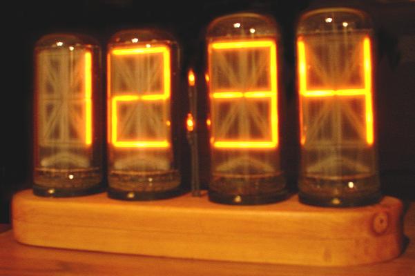
I also found out that the circuitry draws a good amount of current so I couldn't simply obtain low voltage from the voltage doubler and regulate it for the low voltage supply like I could in my first two nixie clocks. I had to use a very small 8-volt transformer that just barely fits inside the case to supply the low voltage power. Anyway, on to the pictures.
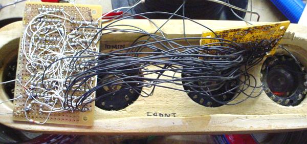
Assembly and Testing
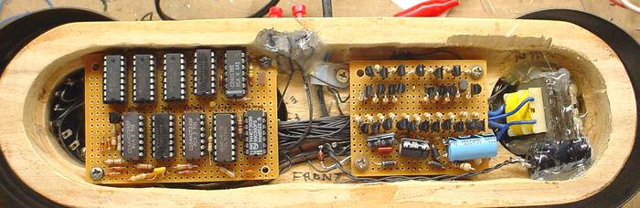
Completed view of assembly bottom view
Back to Top